Datasheet 搜索 > National > CD4046BM 数据手册 > CD4046BM 数据手册 1/14 页


¥ 0
CD4046BM 数据手册 - National
制造商:
National
Pictures:
3D模型
符号图
焊盘图
引脚图
产品图
页面导航:
导航目录
CD4046BM数据手册
Page:
of 14 Go
若手册格式错乱,请下载阅览PDF原文件
TL/F/5968
CD4046BM/CD4046BC Micropower Phase-Locked Loop
November 1995
CD4046BM/CD4046BC Micropower Phase-Locked Loop
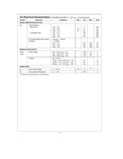
General Description
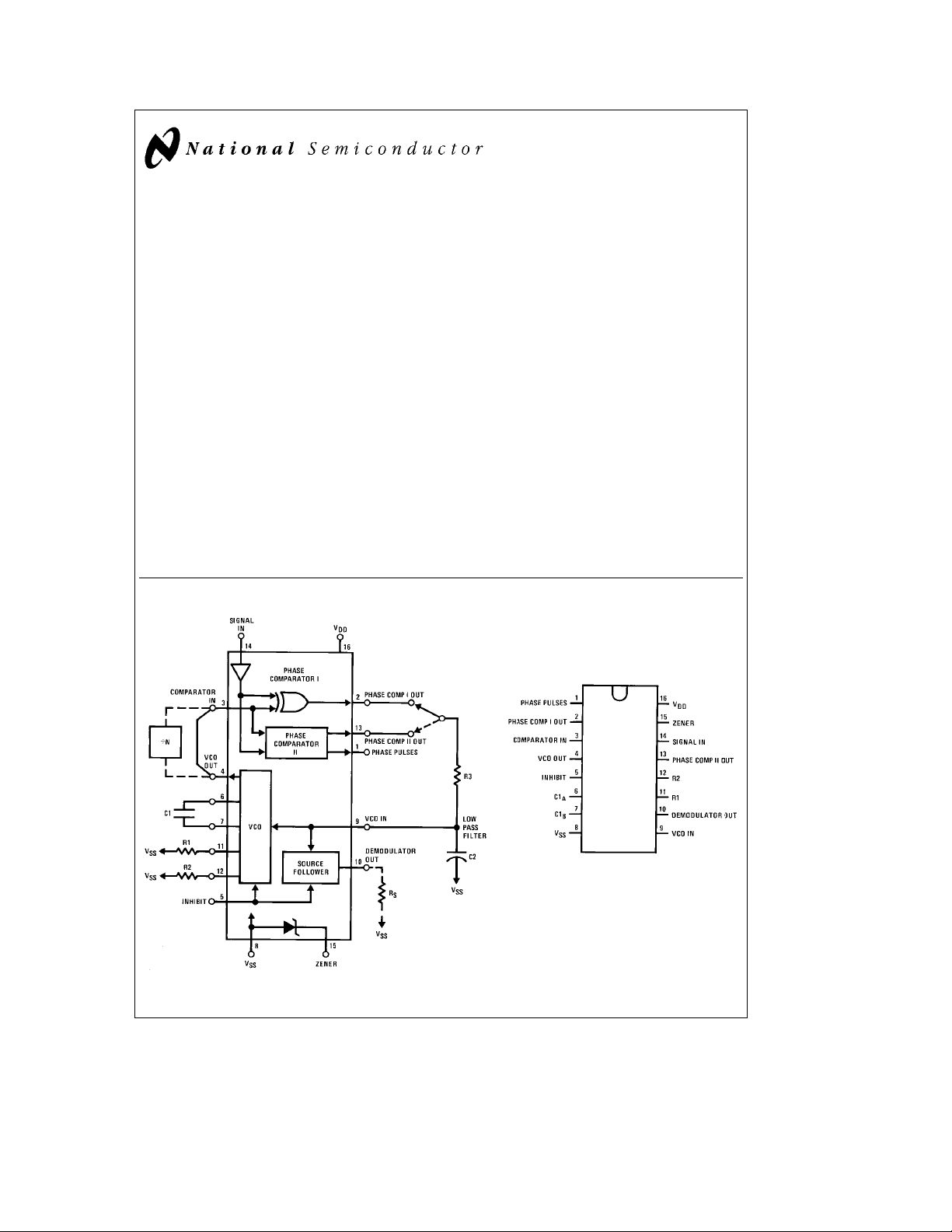
The CD4046B micropower phase-locked loop (PLL) con-
sists of a low power, linear, voltage-controlled oscillator
(VCO), a source follower, a zener diode, and two phase
comparators. The two phase comparators have a common
signal input and a common comparator input. The signal
input can be directly coupled for a large voltage signal, or
capacitively coupled to the self-biasing amplifier at the sig-
nal input for a small voltage signal.
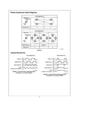
Phase comparator I, an exclusive OR gate, provides a digital
error signal (phase comp. I Out) and maintains 90
§
phase
shifts at the VCO center frequency. Between signal input
and comparator input (both at 50% duty cycle), it may lock
onto the signal input frequencies that are close to harmon-
ics of the VCO center frequency.
Phase comparator II is an edge-controlled digital memory
network. It provides a digital error signal (phase comp. II
Out) and lock-in signal (phase pulses) to indicate a locked
condition and maintains a 0
§
phase shift between signal in-
put and comparator input.
The linear voltage-controlled oscillator (VCO) produces an
output signal (VCO Out) whose frequency is determined by
the voltage at the VCO
IN
input, and the capacitor and resis-
tors connected to pin C1
A
,C1
B
, R1 and R2.
The source follower output of the VCO
IN
(demodulator Out)
is used with an external resistor of 10 kX or more.
The INHIBIT input, when high, disables the VCO and source
follower to minimize standby power consumption. The zener
diode is provided for power supply regulation, if necessary.
Features
Y
Wide supply voltage range 3.0V to 18V
Y
Low dynamic 70 mW (typ.) at
power consumption f
o
e
10 kHz, V
DD
e
5V
Y
VCO frequency 1.3 MHz (typ.) at V
DD
e
10V
Y
Low frequency drift 0.06%/
§
CatV
DD
e
10V
with temperature
Y
High VCO linearity 1% (typ.)
Applications
Y
FM demodulator and modulator
Y
Frequency synthesis and multiplication
Y
Frequency discrimination
Y
Data synchronization and conditioning
Y
Voltage-to-frequency conversion
Y
Tone decoding
Y
FSK modulation
Y
Motor speed control
Block & Connection Diagrams
TL/F/5968– 1
FIGURE 1
Dual-In-Line Package
TL/F/5968– 2
Top View
Order Number CD4046B
C
1995 National Semiconductor Corporation RRD-B30M115/Printed in U. S. A.
器件 Datasheet 文档搜索
AiEMA 数据库涵盖高达 72,405,303 个元件的数据手册,每天更新 5,000 多个 PDF 文件
