Datasheet 搜索 > 多工器 > TI(德州仪器) > CD4051BM 数据手册 > CD4051BM 数据手册 1/38 页
 器件3D模型
¥ 0.893
CD4051BM 数据手册 - TI(德州仪器)
制造商:
TI(德州仪器)
分类:
多工器
封装:
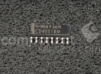
SOIC-16
描述:
TEXAS INSTRUMENTS CD4051BM 芯片, 4000系列 CMOS逻辑器件
Pictures:
3D模型
符号图
焊盘图
引脚图
产品图
页面导航:
引脚图在P3P4Hot
典型应用电路图在P1P19P20
原理图在P16P17
封装尺寸在P23P24P25P26P28P29P30
标记信息在P23P24P25P26
封装信息在P22P23P24P25P26P27P28P29P30
技术参数、封装参数在P5
应用领域在P1P27P38
电气规格在P6P7P8P9P20
导航目录
CD4051BM数据手册
Page:
of 38 Go
若手册格式错乱,请下载阅览PDF原文件
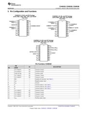
INH
C B A
0 0 0
0 0 1
0 1 0
0 1 1
1 0 0
1 0 1
1 1 0
1 1 1
Ch 0
Ch 1
Ch 2
Ch 3
Ch 4
Ch 5
Ch 6
Ch 7
C B A
COM
ax
ay
bx
by
cx
cy
ax OR ay
bx OR by
cx OR cy
A
B
C
A
B
C
INH
INH
X COM
Y COM
B A
0 0
0 1
1 0
1 1
Ch X0
Ch Y0
Ch X1
Ch Y1
Ch X2
Ch Y2
Ch X3
Ch Y3
AB
CD4051B
CD4052B
CD4053B
Product
Folder
Sample &
Buy
Technical
Documents
Tools &
Software
Support &
Community
CD4051B
,
CD4052B
,
CD4053B
SCHS047H –AUGUST 1998–REVISED APRIL 2015
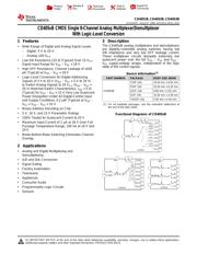
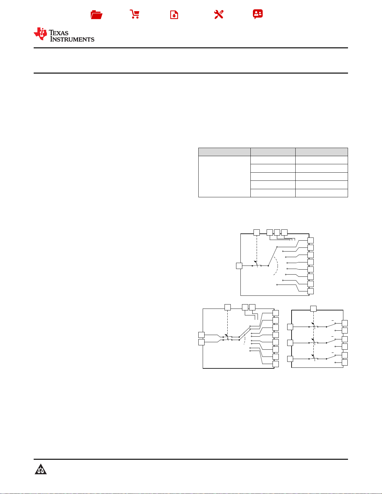
CD405xB CMOS Single 8-Channel Analog Multiplexer/Demultiplexer
With Logic-Level Conversion
1 Features 3 Description
The CD405xB analog multiplexers and demuliplexers
1
• Wide Range of Digital and Analog Signal Levels
are digitally-controlled analog switches having low
– Digital: 3 V to 20 V
ON impedance and very low OFF leakage current.
– Analog: ≤20 V
P-P
These multiplexer circuits dissipate extremely low
quiescent power over the full V
DD
– V
SS
and V
DD
–
• Low ON Resistance,125 Ω (Typical) Over 15 V
P-P
V
EE
supply-voltage ranges, independent of the logic
Signal Input Range for V
DD
– V
EE
= 18 V
state of the control signals.
• High OFF Resistance, Channel Leakage of ±100
pA (Typical) at V
DD
– V
EE
= 18 V
Device Information
(1)
• Logic-Level Conversion for Digital Addressing
PART NUMBER PACKAGE BODY SIZE (NOM)
Signals of 3 V to 20 V (V
DD
– V
SS
= 3 V to 20 V)
CDIP (16) 19.50 mm × 6.92 mm
to Switch Analog Signals to 20 V
P-P
(V
DD
– V
EE
=
PDIP (16) 19.30 mm × 6.35 mm
20 V) Matched Switch Characteristics, r
ON
= 5 Ω
CD405xB SOIC (16) 9.90 mm × 3.91 mm
(Typical) for V
DD
– V
EE
= 15 V Very Low Quiescent
SOP (16) 10.30 mm × 5.30 mm
Power Dissipation Under All Digital-Control Input
TSSOP (16) 5.00 mm × 4.40 mm
and Supply Conditions, 0.2 µW (Typical) at V
DD
–
V
SS
= V
DD
– V
EE
= 10 V
(1) For all available packages, see the orderable addendum at
the end of the data sheet.
• Binary Address Decoding on Chip
• 5 V, 10 V, and 15 V Parametric Ratings
Functional Diagrams of CD405xB
• 100% Tested for Quiescent Current at 20 V
• Maximum Input Current of 1 µA at 18 V Over Full
Package Temperature Range, 100 nA at 18 V and
25°C
• Break-Before-Make Switching Eliminates Channel
Overlap
2 Applications
• Analog and Digital Multiplexing and
Demultiplexing
• A/D and D/A Conversion
• Signal Gating
• Factory Automation
• Televisions
• Appliances
• Consumer Audio
• Programmable Logic Circuits
• Sensors
1
An IMPORTANT NOTICE at the end of this data sheet addresses availability, warranty, changes, use in safety-critical applications,
intellectual property matters and other important disclaimers. PRODUCTION DATA.
器件 Datasheet 文档搜索
AiEMA 数据库涵盖高达 72,405,303 个元件的数据手册,每天更新 5,000 多个 PDF 文件
