Datasheet 搜索 > 接口芯片 > TI(德州仪器) > CD4051BM96G3 数据手册 > CD4051BM96G3 数据手册 20/38 页
 器件3D模型
¥ 1.968
CD4051BM96G3 数据手册 - TI(德州仪器)
制造商:
TI(德州仪器)
分类:
接口芯片
封装:
SOIC-16
描述:
CMOS模拟多路复用器/多路解复用器与逻辑电平转换 CMOS Analog Multiplexers/Demultiplexers with Logic Level Conversion
Pictures:
3D模型
符号图
焊盘图
引脚图
产品图
页面导航:
引脚图在P3P4Hot
典型应用电路图在P1P19P20
原理图在P16P17
封装尺寸在P23P24P25P26P28P29P30
标记信息在P23P24P25P26
封装信息在P22P23P24P25P26P27P28P29P30
技术参数、封装参数在P5
应用领域在P1P27P38
电气规格在P6P7P8P9P20
导航目录
CD4051BM96G3数据手册
Page:
of 38 Go
若手册格式错乱,请下载阅览PDF原文件
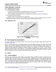
-6 -4 -2 0 2 4 6
V , INPUT SIGNAL VOLTAGE (V)
IS
V
OS
, OUTPUT SIGNAL VOLTAGE (V)
-6
-4
-2
0
2
4
6
V = 5V
DD
V = 0V
SS
V = -5V
EE
T = 25 C
A
o
R = 100k , R = 10k
L L
Ω Ω
100Ω
500Ω
1kΩ
CD4051B
,
CD4052B
,
CD4053B
SCHS047H –AUGUST 1998–REVISED APRIL 2015
www.ti.com
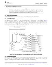
Typical Application (continued)
9.2.2 Detailed Design Procedure
1. Recommended Input Conditions
– For switch time specifications, see propagation delay times in Electrical Characteristics.
– Inputs should not be pushed more than 0.5 V above V
DD
or below V
EE
.
– For input voltage level specifications for control inputs, see V
IH
and V
IL
in Electrical Characteristics.
2. Recommended Output Conditions
– Outputs should not be pulled above V
DD
or below V
EE
.
3. Input/output current consideration: The CD405xB series of parts do not have internal current drive circuitry
and thus cannot sink or source current. Any current will be passed through the device.
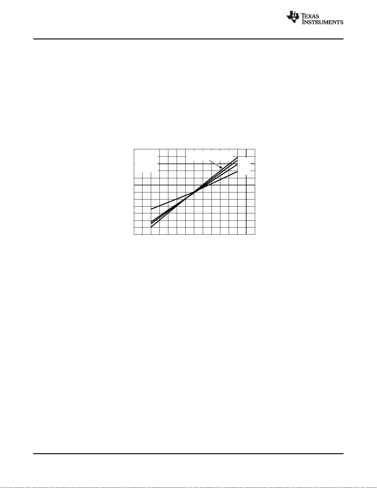
9.2.3 Application Curve
Figure 29. ON Characteristics for 1 of 8 Channels
(CD4051B)
10 Power Supply Recommendations
The power supply can be any voltage between the minimum and maximum supply voltage rating located in the
Electrical Characteristics.
Each V
CC
terminal should have a good bypass capacitor to prevent power disturbance. For devices with a single
supply, a 0.1-μF bypass capacitor is recommended. If there are multiple pins labeled V
CC
, then a 0.01-μF or
0.022-μF capacitor is recommended for each V
CC
because the V
CC
pins will be tied together internally. For
devices with dual supply pins operating at different voltages, for example V
CC
and V
DD
, a 0.1-µF bypass
capacitor is recommended for each supply pin. It is acceptable to parallel multiple bypass capacitors to reject
different frequencies of noise. 0.1-μF and 1-μF capacitors are commonly used in parallel. The bypass capacitor
should be installed as close to the power terminal as possible for best results.
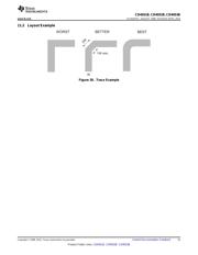
11 Layout
11.1 Layout Guidelines
Reflections and matching are closely related to loop antenna theory, but different enough to warrant their own
discussion. When a PCB trace turns a corner at a 90° angle, a reflection can occur. This is primarily due to the
change of width of the trace. At the apex of the turn, the trace width is increased to 1.414 times its width. This
upsets the transmission line characteristics, especially the distributed capacitance and self–inductance of the
trace — resulting in the reflection. It is a given that not all PCB traces can be straight, and so they will have to
turn corners. Figure 30 shows progressively better techniques of rounding corners. Only the last example
maintains constant trace width and minimizes reflections.
20 Submit Documentation Feedback Copyright © 1998–2015, Texas Instruments Incorporated
Product Folder Links: CD4051B CD4052B CD4053B
器件 Datasheet 文档搜索
AiEMA 数据库涵盖高达 72,405,303 个元件的数据手册,每天更新 5,000 多个 PDF 文件
