Datasheet 搜索 > 接口芯片 > TI(德州仪器) > CD4052BM96G4 数据手册 > CD4052BM96G4 数据手册 5/38 页
 器件3D模型
¥ 4.678
CD4052BM96G4 数据手册 - TI(德州仪器)
制造商:
TI(德州仪器)
分类:
接口芯片
封装:
SOIC-16
描述:
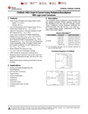
CMOS模拟多路复用器/多路解复用器与逻辑电平转换 CMOS Analog Multiplexers/Demultiplexers with Logic Level Conversion
Pictures:
3D模型
符号图
焊盘图
引脚图
产品图
页面导航:
引脚图在P3P4Hot
典型应用电路图在P1P19P20
原理图在P16P17
封装尺寸在P23P24P25P26P28P29P30
标记信息在P23P24P25P26
封装信息在P22P23P24P25P26P27P28P29P30
技术参数、封装参数在P5
应用领域在P1P27
电气规格在P6P7P8P9P20
导航目录
CD4052BM96G4数据手册
Page:
of 38 Go
若手册格式错乱,请下载阅览PDF原文件
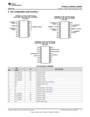
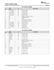
CD4051B
,
CD4052B
,
CD4053B
www.ti.com
SCHS047H –AUGUST 1998–REVISED APRIL 2015
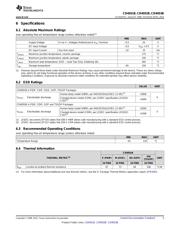
6 Specifications
6.1 Absolute Maximum Ratings
over operating free-air temperature range (unless otherwise noted)
(1)
MIN MAX UNIT
Supply Voltage V+ to V-, Voltages Referenced to V
SS
Terminal –0.5 20 V
DC Input Voltage –0.5 V
DD
+ 0.5 V
DC Input Current Any One Input –10 10 mA
T
JMAX1
Maximum junction temperature, ceramic package 175 °C
T
JMAX2
Maximum junction temperature, plastic package 150 °C
T
LMAX
Maximum lead temperature, SOIC - Lead Tips Only, Soldering 10s 265 °C
T
stg
Storage temperature –65 150 °C
(1) Stresses beyond those listed under Absolute Maximum Ratings may cause permanent damage to the device. These are stress ratings
only, which do not imply functional operation of the device at these or any other conditions beyond those indicated under Recommended
Operating Conditions. Exposure to absolute-maximum-rated conditions for extended periods may affect device reliability.
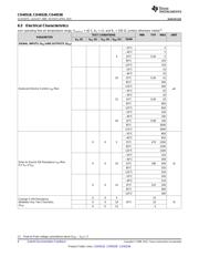
6.2 ESD Ratings
VALUE UNIT
CD4051B in PDIP, CDIP, SOIC, SOP, TSSOP Packages
Human-body model (HBM), per ANSI/ESDA/JEDEC JS-001
(1)
+3000
V
(ESD)
Electrostatic discharge V
Charged-device model (CDM), per JEDEC specification JESD22-
+2000
C101
(2)
CD4053B in PDIP, CDIP, SOP and TSSOP Packages
Human-body model (HBM), per ANSI/ESDA/JEDEC JS-001
(1)
+2500
V
(ESD)
Electrostatic discharge V
Charged-device model (CDM), per JEDEC specification JESD22-
+1500
C101
(2)
(1) JEDEC document JEP155 states that 500-V HBM allows safe manufacturing with a standard ESD control process.
(2) JEDEC document JEP157 states that 250-V CDM allows safe manufacturing with a standard ESD control process.
6.3 Recommended Operating Conditions
over operating free-air temperature range (unless otherwise noted)
MIN MAX UNIT
Temperature Range –55 125 °C
6.4 Thermal Information
CD405xB
PW
THERMAL METRIC
(1)
E (PDIP) M (SOIC) NS (SOP) UNIT
(TSSOP)
16 PINS 16 PINS 16 PINS 16 PINS
R
θJA
Junction-to-ambient thermal resistance 67 73 64 108 °C/W
(1) For more information about traditional and new thermal metrics, see the IC Package Thermal Metrics application report, SPRA953.
Copyright © 1998–2015, Texas Instruments Incorporated Submit Documentation Feedback 5
Product Folder Links: CD4051B CD4052B CD4053B
器件 Datasheet 文档搜索
AiEMA 数据库涵盖高达 72,405,303 个元件的数据手册,每天更新 5,000 多个 PDF 文件
