Datasheet 搜索 > 逻辑控制器 > TI(德州仪器) > CD74AC139M 数据手册 > CD74AC139M 数据手册 2/14 页
 器件3D模型
¥ 1.235
CD74AC139M 数据手册 - TI(德州仪器)
制造商:
TI(德州仪器)
分类:
逻辑控制器
封装:
SOIC-16
描述:
TEXAS INSTRUMENTS CD74AC139M 逻辑芯片, 译码器/信号分离器, 双路, 2-4线, 16SOIC
Pictures:
3D模型
符号图
焊盘图
引脚图
产品图
页面导航:
导航目录
CD74AC139M数据手册
Page:
of 14 Go
若手册格式错乱,请下载阅览PDF原文件
CD54AC139, CD74AC139
DUAL 2-LINE TO 4-LINE DECODERS/DEMULTIPLEXERS
SCHS332 – MARCH 2003
2
POST OFFICE BOX 655303 • DALLAS, TEXAS 75265
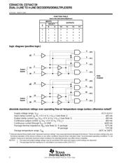
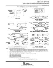
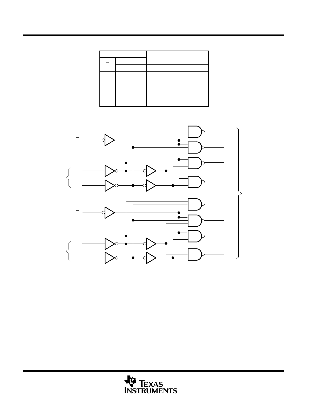
FUNCTION TABLE
(each decoder/demultiplexer)
INPUTS
OUTPUTS
G
SELECT
OUTPUTS
G
B A Y0 Y1 Y2 Y3
H X X H H H H
L L LLHHH
L L HHLHH
L H LHHLH
L H H H H H L
logic diagram (positive logic)
Select
Inputs
Select
Inputs
2B
2A
2G
1B
1A
1G
Data
Outputs
2Y3
2Y2
2Y1
2Y0
1Y3
1Y2
1Y1
1Y0
1
2
3
15
14
13
4
5
6
7
12
11
10
9
absolute maximum ratings over operating free-air temperature range (unless otherwise noted)
†
Supply voltage range, V
CC
–0.5 V to 6 V. . . . . . . . . . . . . . . . . . . . . . . . . . . . . . . . . . . . . . . . . . . . . . . . . . . . . . . . . .
Input clamp current, I
IK
(V
I
< 0 V or V
I
> V
CC
) (see Note 1) ±20 mA. . . . . . . . . . . . . . . . . . . . . . . . . . . . . . . . . . .
Output clamp current, I
OK
(V
O
< 0 V or V
O
> V
CC
) (see Note 1) ±50 mA. . . . . . . . . . . . . . . . . . . . . . . . . . . . . .
Continuous output current, I
O
(V
O
> 0 V or V
O
< V
CC
) ±50 mA. . . . . . . . . . . . . . . . . . . . . . . . . . . . . . . . . . . . . . .
Continuous current through V
CC
or GND ±100 mA. . . . . . . . . . . . . . . . . . . . . . . . . . . . . . . . . . . . . . . . . . . . . . . . . .
Package thermal impedance, θ
JA
(see Note 2): E package 67°C/W. . . . . . . . . . . . . . . . . . . . . . . . . . . . . . . . . . .
M package 73°C/W. . . . . . . . . . . . . . . . . . . . . . . . . . . . . . . . . .
Storage temperature range, T
stg
–65°C to 150°C. . . . . . . . . . . . . . . . . . . . . . . . . . . . . . . . . . . . . . . . . . . . . . . . . . .
†
Stresses beyond those listed under “absolute maximum ratings” may cause permanent damage to the device. These are stress ratings only, and
functional operation of the device at these or any other conditions beyond those indicated under “recommended operating conditions” is not
implied. Exposure to absolute-maximum-rated conditions for extended periods may affect device reliability.
NOTES: 1. The input and output voltage ratings may be exceeded if the input and output current ratings are observed.
2. The package thermal impedance is calculated in accordance with JESD 51-7.
器件 Datasheet 文档搜索
AiEMA 数据库涵盖高达 72,405,303 个元件的数据手册,每天更新 5,000 多个 PDF 文件
