Datasheet 搜索 > 时钟发生器 > TI(德州仪器) > CDCE72010RGCT G4 数据手册 > CDCE72010RGCT G4 数据手册 1/77 页

¥ 0
CDCE72010RGCT G4 数据手册 - TI(德州仪器)
制造商:
TI(德州仪器)
分类:
时钟发生器
Pictures:
3D模型
符号图
焊盘图
引脚图
产品图
页面导航:
导航目录
CDCE72010RGCT G4数据手册
Page:
of 77 Go
若手册格式错乱,请下载阅览PDF原文件
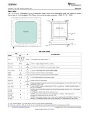
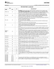
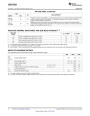
CDCE72010
www.ti.com
SCAS858C –JUNE 2008– REVISED JANUARY 2012
Ten Output High Performance Clock Synchronizer, Jitter Cleaner, and Clock Distributor
Check for Samples: CDCE72010
1
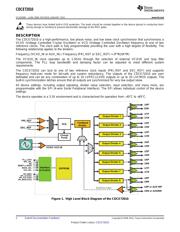
FEATURES
• Wide Charge-Pump Current Range From
200μA to 3mA
• High Performance LVPECL, LVDS, LVCMOS
• Presets Charge-Pump to V
CC_CP
/2 for Fast
PLL Clock Synchronizer
Center-Frequency Setting of VC(X)O,
• Two Reference Clock Inputs (Primary and
Controlled Via the SPI Bus
Secondary Clock) for Redundancy Support
• SERDES Startup Mode (Depending on VCXO
with Manual or Automatic Selection
Range)
• Accepts Two Differential Input (LVPECL or
• Auxiliary Input: Output 9 can Serve as 2nd
LVDS) References up to 500MHz (or Two
VCXO Input to Drive All Outputs or to Serve as
LVCMOS Inputs up to 250MHz) as PLL
PLL Feedback Signal
Reference
• RESET or HOLD Input Pin to Serve as Reset or
• VCXO_IN Clock is Synchronized to One of Two
Hold Functions
Reference Clocks
• REFERENCE SELECT for Manual Select
• VCXO_IN Frequencies up to 1.5GHz (LVPECL)
Between Primary and Secondary Reference
800MHz for LVDS and 250MHz for LVCMOS
Clocks
Level Signaling
• POWER DOWN (PD) to Put Device in Standby
• Outputs Can be a Combination of LVPECL,
Mode
LVDS, and LVCMOS (Up to 10 Differential
LVPECL or LVDS Outputs or up to 20 LVCMOS
• Analog and Digital PLL Lock Indicator
Outputs), Output 9 can be Converted to an
• Internally Generated VBB Bias Voltages for
Auxiliary Input as a 2nd VC(X)O.
Single-Ended Input Signals
• Output Divider is Selectable to Divide by 1, 2,
• Frequency Hold-Over Mode Activated by
3, 4, 5, 6, 8, 10, 12, 16, 18, 20, 24, 28, 30, 32, 36,
HOLD Pin or SPI Bus to Improve Fail-Safe
40, 42, 48, 50, 56, 60, 64, 70, or 80 On Each
Operation
Output Individually up to Eight Dividers.
• Input to All Outputs Skew Control
(Except for Output 0 and 9, Output 0 Follows
• Individual Skew Control for Each Output with
Output 1 Divider and Output 9 Follows Output
Each Output Divider
8 Divider)
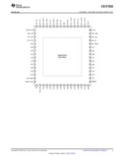
• Packaged in a QFN-64 Package
• SPI Controllable Device Setting
• ESD Protection Exceeds 2kV HBM
• Individual Output Enable Control via SPI
• Industrial Temperature Range of –40°C to 85°
Interface
• Integrated On-Chip Non-Volatile Memory
APPLICATIONS
(EEPROM) to Store Settings without the Need
to Apply High Voltage to the Device • Low Jitter Clock Driver for High-End Telecom
and Wireless Applications
• Optional Configuration Pins to Select Between
Two Default Settings Stored in EEPROM • High Precision Test Equipment
• Efficient Jitter Cleaning from Low PLL Loop
Bandwidth
• Very Low Phase Noise PLL Core
• Programmable Phase Offset (Input Reference
to Outputs)
1
Please be aware that an important notice concerning availability, standard warranty, and use in critical applications of Texas
Instruments semiconductor products and disclaimers thereto appears at the end of this data sheet.
PRODUCTION DATA information is current as of publication date.
Copyright © 2008–2012, Texas Instruments Incorporated
Products conform to specifications per the terms of the Texas
Instruments standard warranty. Production processing does not
necessarily include testing of all parameters.
器件 Datasheet 文档搜索
AiEMA 数据库涵盖高达 72,405,303 个元件的数据手册,每天更新 5,000 多个 PDF 文件
