Datasheet 搜索 > 时钟信号器件 > Cypress Semiconductor(赛普拉斯) > CY25811ZXC 数据手册 > CY25811ZXC 数据手册 6/13 页
 器件3D模型
¥ 2.542
CY25811ZXC 数据手册 - Cypress Semiconductor(赛普拉斯)
制造商:
Cypress Semiconductor(赛普拉斯)
分类:
时钟信号器件
封装:
TSSOP-8
描述:
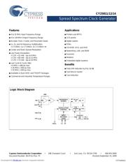
扩频时钟发生器 Spread Spectrum Clock Generator
Pictures:
3D模型
符号图
焊盘图
引脚图
产品图
页面导航:
导航目录
CY25811ZXC数据手册
Page:
of 13 Go
若手册格式错乱,请下载阅览PDF原文件
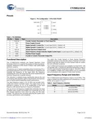
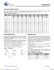
CY25811/12/14
Document Number: 38-07112 Rev. *H Page 6 of 13
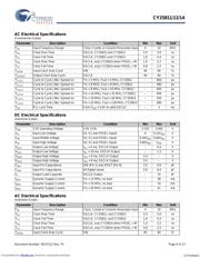
AC Electrical Specifications
(Commercial Grade)
Parameter Description Condition Min Max Unit
F
IN
Input Frequency Range Clock, Crystal, or Ceramic Resonator Input 4 32 MHz
T
R1
Clock Rise Time SSCLK, CY25811 and CY25812 2.0 5.0 ns
T
F1
Clock Fall Time SSCLK, CY25811 and CY25812 1.6 4.4 ns
T
R2
Clock Rise Time SSCLK, only CY25814 when FRSEL = M 1.0 2.2 ns
T
F2
Clock Fall Time SSCLK, only CY25814 when FRSEL = M 0.8 2.2 ns
T
DCIN
Input Clock Duty Cycle XIN 40 60 %
T
DCOUT
Output Clock Duty Cycle SSCLK 40 60 %
T
CCJ1
Cycle to Cycle Jitter, Spread on Fin = 4 MHz, Fout = 4 MHz, CY25811 – 800 ps
T
CCJ2
Cycle to Cycle Jitter, Spread on Fin = 8 MHZ, Fout = 8 MHz, CY25811 – 480 ps
T
CCJ3
Cycle to Cycle Jitter, Spread on Fin = 8 MHz, Fout = 16 MHz, CY25812 – 400 ps
T
CCJ4
Cycle to Cycle Jitter, Spread on Fin = 16 MHz, Fout = 32 MHz, CY25812 – 450 ps
T
CCJ5
Cycle to Cycle Jitter, Spread on Fin = 16 MHz, Fout = 64 MHz, CY25814 – 550 ps
T
CCJ6
Cycle to Cycle Jitter, Spread on Fin = 32 MHz, Fout = 128 MHz, CY25814 – 380 ps
T
SU
PLL Lock Time From V
DD
= 3.0V to valid SSCLK – 3 ms
DC Electrical Specifications
(Industrial Grade)
Parameter Description Condition Min Max Unit
V
DD
3.3V Operating Voltage 3.3V ± 5% 3.135 3.465 V
V
IL
Input Low Voltage S0, S1 and FRSEL Inputs 0 0.13V
DD
V
V
IM
Input Middle Voltage S0, S1 and FRSEL Inputs 0.40V
DD
0.60V
DD
V
V
IH
Input High Voltage S0, S1 and FRSEL Inputs 0.85V
DD
V
DD
V
V
OL1
Output Low Voltage I
OL
= 4 ma, SSCLK Output – 0.4 V
V
OL2
Output Low Voltage I
OL
= 10 ma, SSCLK Output – 1.2 V
V
OH1
Output High Voltage I
OH
= 4 ma, SSCLK Output 2.4 – V
V
OH2
Output High Voltage I
OH
= 6 ma, SSCLK Output 2.0 – V
C
IN1
Input Pin Capacitance XIN (Pin 1) and XOUT (Pin 8) 3.5 9.0 pF
C
IN2
Input Pin Capacitance All Digital Inputs 2.8 6.0 pF
C
L
Output Load Capacitor SSCLK Output – 15 pF
I
DD1
Dynamic Supply Current Fin = 12 MHz, no load – 28 mA
I
DD2
Dynamic Supply Current Fin = 24 MHz, no load – 33 mA
I
DD3
Dynamic Supply Current Fin = 32 MHz, no load – 41 mA
AC Electrical Specifications
(Industrial Grade)
Parameter Description Condition Min Max Unit
F
IN
Input Frequency Range Clock, Crystal or Ceramic Resonator Input 4 32 MHz
T
R1
Clock Rise Time SSCLK, CY25811, and CY25812 2.0 5.0 ns
T
F1
Clock Fall Time SSCLK, CY25811, and CY25812 1.6 4.4 ns
T
R2
Clock Rise Time SSCLK, only CY25814 when FRSEL = M 1.0 2.2 ns
T
F2
Clock Fall Time SSCLK, only CY25814 when FRSEL = M 0.8 2.2 ns
T
DCIN
Input Clock Duty Cycle XIN 40 60 %
[+] Feedback
Downloaded from Elcodis.com electronic components distributor
器件 Datasheet 文档搜索
AiEMA 数据库涵盖高达 72,405,303 个元件的数据手册,每天更新 5,000 多个 PDF 文件
