Datasheet 搜索 > RAM芯片 > Cypress Semiconductor(赛普拉斯) > CY62256VNLL-70ZRXI 数据手册 > CY62256VNLL-70ZRXI 数据手册 1/17 页
 器件3D模型
¥ 3.101
CY62256VNLL-70ZRXI 数据手册 - Cypress Semiconductor(赛普拉斯)
制造商:
Cypress Semiconductor(赛普拉斯)
分类:
RAM芯片
封装:
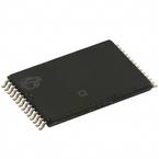
TSSOP-28
描述:
CY62256VN 系列 256 Kb (32 K x 8) 3 V 70 ns 静态RAM - TSOP-28
Pictures:
3D模型
符号图
焊盘图
引脚图
产品图
页面导航:

导航目录
CY62256VNLL-70ZRXI数据手册
Page:
of 17 Go
若手册格式错乱,请下载阅览PDF原文件
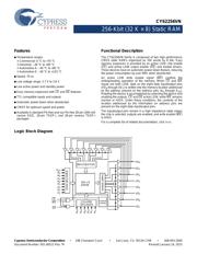
CY62256VN
256-Kbit (32 K × 8) Static RAM
Cypress Semiconductor Corporation • 198 Champion Court • San Jose, CA 95134-1709 • 408-943-2600
Document Number: 001-06512 Rev. *H Revised January 16, 2015
256-Kbit (32 K × 8) Static RAM
Features
■ Temperature ranges
❐ Commercial: 0 °C to +70 °C
❐ Industrial: –40 °C to +85 °C
❐ Automotive-A: –40 °C to +85 °C
❐ Automotive-E: –40 °C to +125 °C
■ Speed: 70 ns
■ Low voltage range: 2.7 V to 3.6 V
■ Low active power and standby power
■ Easy memory expansion with CE and OE features
■ TTL compatible inputs and outputs
■ Automatic power-down when deselected
■ CMOS for optimum speed and power
■ Available in standard Pb-free and non Pb-free 28-pin (300-mil)
narrow SOIC, 28-pin TSOP-I, and 28-pin reverse TSOP-I
packages
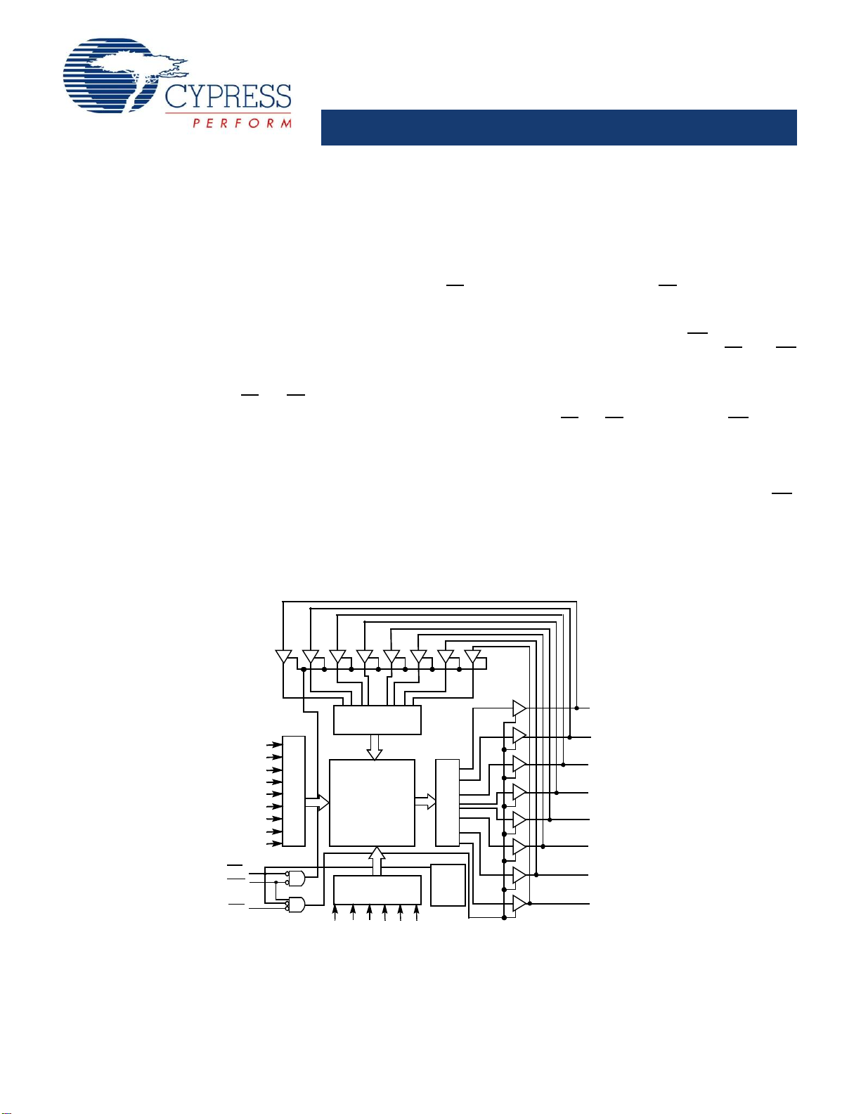
Functional Description
The CY62256VN family is composed of two high performance
CMOS static RAM’s organized as 32K words by 8 bits. Easy
memory expansion is provided by an active LOW chip enable
(CE
) and active LOW output enable (OE) and tristate drivers.
These devices have an automatic power-down feature, reducing
the power consumption by over 99% when deselected.
An active LOW write enable signal (WE) controls the
writing/reading operation of the memory. When CE
and WE
inputs are both LOW, data on the eight data input/output pins
(I/O
0
through I/O
7
) is written into the memory location addressed
by the address present on the address pins (A
0
through A
14
).
Reading the device is accomplished by selecting the device and
enabling the outputs, CE
and OE active LOW, while WE remains
inactive or HIGH. Under these conditions, the contents of the
location addressed by the information on address pins are
present on the eight data input/output pins.
The input/output pins remain in a high impedance state unless
the chip is selected, outputs are enabled, and write enable (WE
)
is HIGH.
For a complete list of related documentation, click here.
A
9
A
8
A
7
A
6
A
5
A
4
A
3
A
2
COLUMN
DECODER
ROW DECODER
SENSE AMPS
INPUTBUFFER
POWER
DOWN
WE
OE
I/O
0
CE
I/O
1
I/O
2
I/O
3
32K x 8
ARRA
Y
I/O
7
I/O
6
I/O
5
I/O
4
A
10
A
13
A
11
A
12
A
A
14
A
1
0
Logic Block Diagram
器件 Datasheet 文档搜索
AiEMA 数据库涵盖高达 72,405,303 个元件的数据手册,每天更新 5,000 多个 PDF 文件
