Datasheet 搜索 > 存储芯片 > Cypress Semiconductor(赛普拉斯) > CY7C1049B-15VC 数据手册 > CY7C1049B-15VC 数据手册 1/10 页
 器件3D模型
¥ 30.669
CY7C1049B-15VC 数据手册 - Cypress Semiconductor(赛普拉斯)
制造商:
Cypress Semiconductor(赛普拉斯)
分类:
存储芯片
封装:
SOJ-36
描述:
512K ×8静态RAM 512K x 8 Static RAM
Pictures:
3D模型
符号图
焊盘图
引脚图
产品图
页面导航:
导航目录
CY7C1049B-15VC数据手册
Page:
of 10 Go
若手册格式错乱,请下载阅览PDF原文件
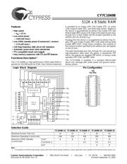
512K x 8 Static RAM
CY7C1049B
Cypress Semiconductor Corporation • 3901 North First Street • San Jose • CA 95134 • 408-943-2600
Document #: 38-05169 Rev. *A Revised September 13, 2002
049B
Features
• High speed
—t
AA
= 12 ns
• Low active power
—1320 mW (max.)
• Low CMOS standby power (Commercial L version)
—2.75 mW (max.)
• 2.0V Data Retention (400 µW at 2.0V retention)
• Automatic power-down when deselected
• TTL-compatible inputs and outputs
• Easy memory expansion with CE
and OE features
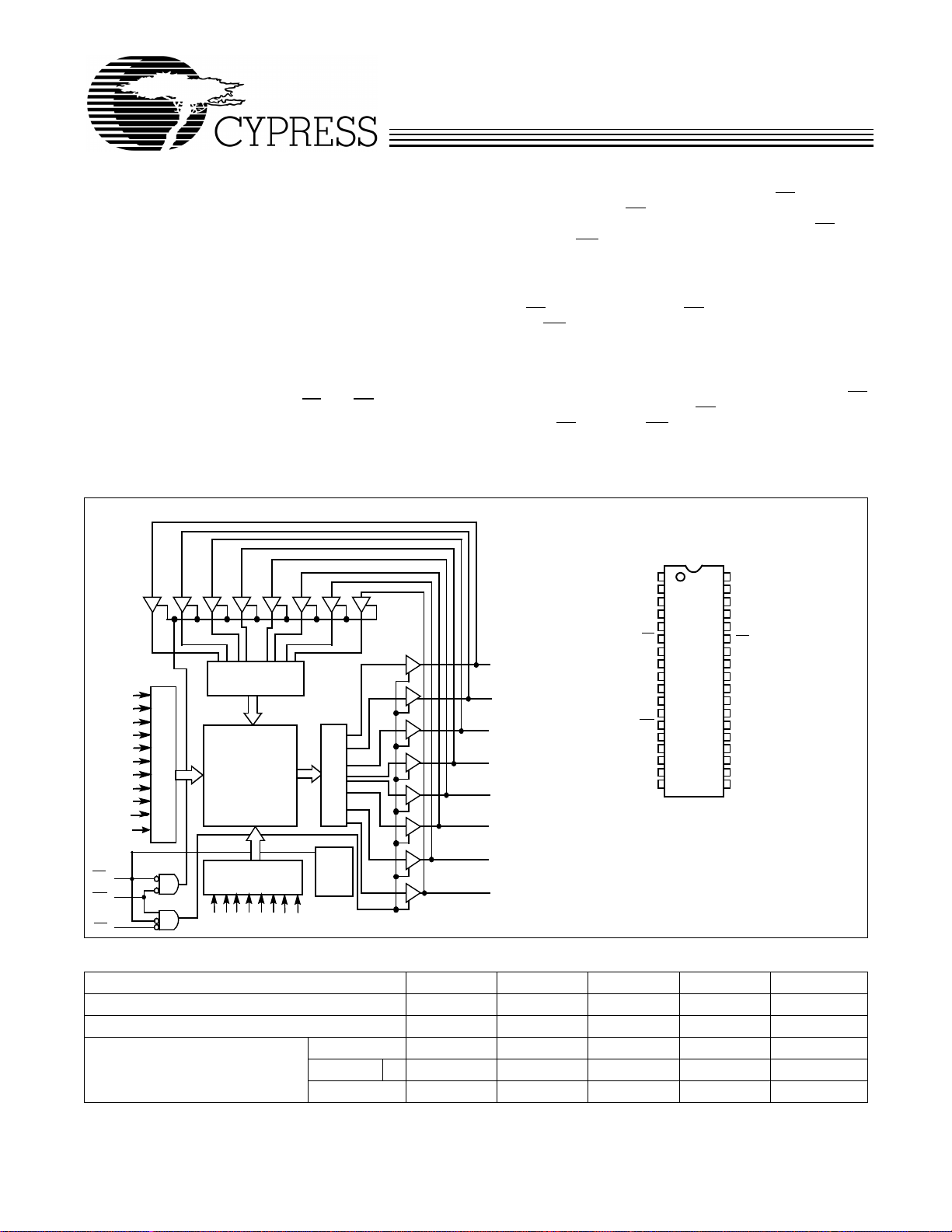
Functional Description
[1]
The CY7C1049B is a high-performance CMOS static RAM or-
ganized as 524,288 words by 8 bits. Easy memory expansion
is provided by an active LOW Chip Enable (CE
), an active
LOW Output Enable (OE
), and three-state drivers. Writing to
the device is accomplished by taking Chip Enable (CE
) and
Write Enable (WE
) inputs LOW. Data on the eight I/O pins (I/O
0
through I/O
7
) is then written into the location specified on the
address pins (A
0
through A
18
).
Reading from the device is accomplished by taking Chip En-
able (CE
) and Output Enable (OE) LOW while forcing Write
Enable (WE
) HIGH. Under these conditions, the contents of
the memory location specified by the address pins will appear
on the I/O pins.
The eight input/output pins (I/O
0
through I/O
7
) are placed in a
high-impedance state when the device is deselected (CE
HIGH), the outputs are disabled (OE HIGH), or during a write
operation (CE
LOW, and WE LOW).
The CY7C1049B is available in a standard 400-mil-wide
36-pin SOJ package with center power and ground (revolu-
tionary) pinout.
Note:
1. For guidelines on SRAM system design, please refer to the ‘System Design Guidelines’ Cypress application note, available on the internet at www.cypress.com.
14
15
Logic Block Diagram Pin Configuration
A
1
A
2
A
3
A
4
A
5
A
6
A
7
A
8
COLUMN
DECODER
ROW DECODER
SENSE AMPS
INPUT BUFFER
POWER
DOWN
WE
OE
I/O
0
I/O
1
I/O
2
I/O
3
512K x 8
ARRAY
I/O
7
I/O
6
I/O
5
I/O
4
A
0
A
11
A
13
A
12
A
CE
A
A
16
A
17
1
2
3
4
5
6
7
8
9
10
11
14
23
24
28
27
26
25
29
32
31
30
Top View
SOJ
12
13
33
36
35
34
16
15
21
22
GND
A
1
A
2
A
3
A
4
A
5
A
6
A
7
A
8
WE
V
CC
A
18
A
15
A
12
A
14
I/O
5
I/O
4
A
9
A
0
I/O
0
I/O
1
I/O
2
OE
A
17
A
16
A
13
CE
A
9
A
18
18
17
19
20
GND
I/O
7
I/O3
I/O
6
V
CC
A
10
A
11
NC
NC
A
10
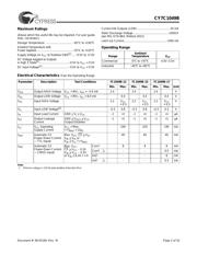
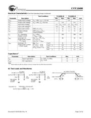
Selection Guide
7C1049B-12 7C1049B-15 7C1049B-17 7C1049B-20 7C1049B-25
Maximum Access Time (ns) 12 15 17 20 25
Maximum Operating Current (mA) 240 220 195 185 180
Maximum CMOS Standby
Current (mA)
Com’l888 8 8
Com’l/Ind’l L- - 0.5 0.5 0.5
Ind’l--- 9 9
器件 Datasheet 文档搜索
AiEMA 数据库涵盖高达 72,405,303 个元件的数据手册,每天更新 5,000 多个 PDF 文件
