Datasheet 搜索 > 微控制器 > Cypress Semiconductor(赛普拉斯) > CY7C68013A-100AXI 数据手册 > CY7C68013A-100AXI 数据手册 29/71 页
 器件3D模型
¥ 57.662
CY7C68013A-100AXI 数据手册 - Cypress Semiconductor(赛普拉斯)
制造商:
Cypress Semiconductor(赛普拉斯)
分类:
微控制器
封装:
TQFP-100
描述:
USB 2.0高速外设控制器,EZ-USB FX2LP系列
Pictures:
3D模型
符号图
焊盘图
引脚图
产品图
页面导航:
引脚图在P16P18P19P20P21P22P23P24P25P26P27P28Hot
原理图在P3
焊盘布局在P64
型号编码规则在P57
封装信息在P15P58
应用领域在P5P6P57
电气规格在P41
型号编号列表在P67

导航目录
CY7C68013A-100AXI数据手册
Page:
of 71 Go
若手册格式错乱,请下载阅览PDF原文件
CY7C68013A, CY7C68014A
CY7C68015A, CY7C68016A
Document Number: 38-08032 Rev. *X Page 29 of 71
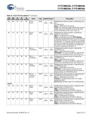
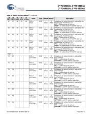
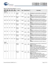
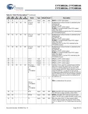
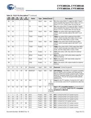
9 8 – – – RDY5 Input N/A N/A RDY5 is a GPIF input signal.
69 54 36 29 7H CTL0 or
FLAGA
O/Z H L Multiplexed pin whose function is selected by the
following bits:
IFCONFIG[1..0].
CTL0 is a GPIF control output.
FLAGA is a programmable slave-FIFO output
status flag signal.
Defaults to programmable for the FIFO selected by
the FIFOADR[1:0] pins.
70 55 37 30 7G CTL1 or
FLAGB
O/Z H L Multiplexed pin whose function is selected by the
following bits:
IFCONFIG[1..0].
CTL1 is a GPIF control output.
FLAGB is a programmable slave-FIFO output
status flag signal.
Defaults to FULL for the FIFO selected by the
FIFOADR[1:0] pins.
71 56 38 31 8H CTL2 or
FLAGC
O/Z H L Multiplexed pin whose function is selected by the
following bits:
IFCONFIG[1..0].
CTL2 is a GPIF control output.
FLAGC is a programmable slave-FIFO output
status flag signal.
Defaults to EMPTY for the FIFO selected by the
FIFOADR[1:0] pins.
66 51 – – – CTL3 O/Z H L CTL3 is a GPIF control output.
67 52 – – – CTL4 Output H L CTL4 is a GPIF control output.
98 76 – – – CTL5 Output H L CTL5 is a GPIF control output.
32 26 20 13 2G IFCLK on
CY7C68013
A
and
CY7C68014
A
-----------------
-
PE0 on
CY7C68015
A
and
CY7C68016
A
I/O/Z
----------
-
I/O/Z
Z
----------
I
Z
----------
Z
Interface Clock, used for synchronously clocking
data into or out of the slave FIFOs. IFCLK also
serves as a timing reference for all slave FIFO
control signals and GPIF. When internal clocking is
used (IFCONFIG.7 = 1) the IFCLK pin can be
configured to output 30/48 MHz by bits IFCONFIG.5
and IFCONFIG.6. IFCLK may be inverted, whether
internally or externally sourced, by setting the bit
IFCONFIG.4 =1.
-------------------------------------------------------------------
----
PE0 is a bidirectional I/O port pin.
28 22 – – – INT4 Input N/A N/A INT4 is the 8051 INT4 interrupt request input signal.
The INT4 pin is edge-sensitive, active HIGH.
106 84 – – – INT5# Input N/A N/A INT5# is the 8051 INT5 interrupt request input
signal. The INT5 pin is edge-sensitive, active LOW.
31 25 – – – T2 Input N/A N/A T2 is the active HIGH T2 input signal to 8051
Timer2, which provides the input to Timer2 when
C/T2 = 1. When C/T2 = 0, Timer2 does not use this
pin.
Table 10. FX2LP Pin Descriptions
[11]
(continued)
128
TQFP
100
TQFP
56
SSOP
56
QFN
56
VFBGA
Name Type Default Reset
[12]
Description
器件 Datasheet 文档搜索
AiEMA 数据库涵盖高达 72,405,303 个元件的数据手册,每天更新 5,000 多个 PDF 文件
