Datasheet 搜索 > 双极性晶体管 > ON Semiconductor(安森美) > D45VH10G 数据手册 > D45VH10G 数据手册 1/6 页

¥ 3.085
D45VH10G 数据手册 - ON Semiconductor(安森美)
制造商:
ON Semiconductor(安森美)
分类:
双极性晶体管
封装:
TO-220-3
描述:
PNP 功率晶体管,ON Semiconductor### 标准带 NSV 前缀的制造商部件号具有汽车资格,符合 AEC-Q101 标准。
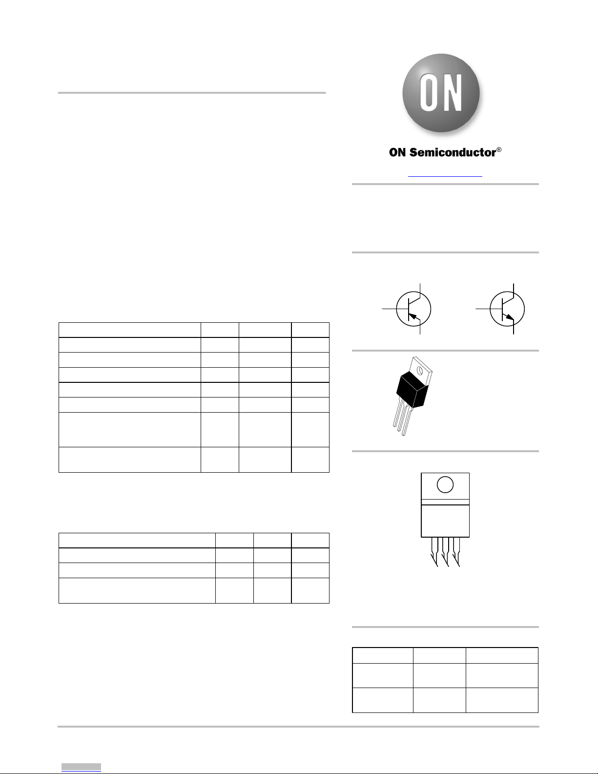
Pictures:
3D模型
符号图
焊盘图
引脚图
产品图
页面导航:
导航目录
D45VH10G数据手册
Page:
of 6 Go
若手册格式错乱,请下载阅览PDF原文件
© Semiconductor Components Industries, LLC, 2014
November, 2014 − Rev. 8
1 Publication Order Number:
D44VH/D
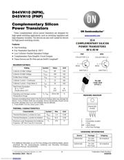
D44VH10(NPN),
D45VH10 (PNP)
Complementary Silicon
Power Transistors
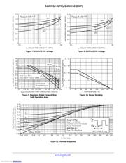
These complementary silicon power transistors are designed for
high−speed switching applications, such as switching regulators and
high frequency inverters. The devices are also well−suited for drivers
for high power switching circuits.
Features
• Fast Switching
• Key Parameters Specified @ 100°C
• Low Collector−Emitter Saturation Voltage
• Complementary Pairs Simplify Circuit Designs
• These Devices are Pb−Free and are RoHS Compliant*
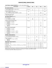
MAXIMUM RATINGS
Rating Symbol Value Unit
Collector−Emitter Voltage V
CEO
80 Vdc
Collector−Emitter Voltage V
CEV
100 Vdc
Emitter Base Voltage V
EB
7.0 Vdc
Collector Current − Continuous I
C
15 Adc
Collector Current − Peak (Note 1) I
CM
20 Adc
Total Power Dissipation
@ T
C
= 25°C
Derate above 25°C
P
D
83
0.67
W
W/°C
Operating and Storage Junction
Temperature Range
T
J
, T
stg
−55 to 150 °C
Stresses exceeding those listed in the Maximum Ratings table may damage the
device. If any of these limits are exceeded, device functionality should not be
assumed, damage may occur and reliability may be affected.
1. Pulse Width ≤ 6.0 ms, Duty Cycle ≤ 50%.
THERMAL CHARACTERISTICS
Characteristic Symbol Max Unit
Thermal Resistance, Junction to Case
R
q
JC
1.5 °C/W
Thermal Resistance, Junction to Ambient
R
q
JA
62.5 °C/W
Maximum Lead Temperature for Soldering
Purposes: 1/8″ from Case for 5 Seconds
T
L
275 °C
*For additional information on our Pb−Free strategy and soldering details, please
download the ON Semiconductor Soldering and Mounting Techniques
Reference Manual, SOLDERRM/D.
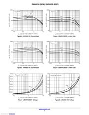
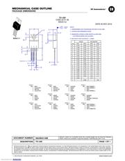
Device Package Shipping
ORDERING INFORMATION
MARKING DIAGRAM
15 A
COMPLEMENTARY SILICON
POWER TRANSISTORS
80 V, 83 W
x = 4 or 5
A = Assembly Location
Y = Year
WW = Work Week
G = Pb−Free Package
D44VH10G TO−220
(Pb−Free)
50 Units/Rail
D45VH10G TO−220
(Pb−Free)
50 Units/Rail
www.onsemi.com
TO−220
CASE 221A
STYLE 1
1
2
3
4
D4xVH10G
AYWW
1
BASE
EMITTER 3
COLLECTOR 2, 4
1
BASE
EMITTER 3
COLLECTOR 2, 4
PNP NPN
Downloaded from Arrow.com.
器件 Datasheet 文档搜索
AiEMA 数据库涵盖高达 72,405,303 个元件的数据手册,每天更新 5,000 多个 PDF 文件
