Datasheet 搜索 > TI(德州仪器) > DAC088S085 数据手册 > DAC088S085 数据手册 4/41 页

¥ 0
DAC088S085 数据手册 - TI(德州仪器)
制造商:
TI(德州仪器)
描述:
具有轨至轨输出的 8 位微功耗八路数模转换器
Pictures:
3D模型
符号图
焊盘图
引脚图
产品图
页面导航:
引脚图在P3P4Hot
典型应用电路图在P25P26P27
原理图在P14P15
封装尺寸在P33P35P36P38
焊盘布局在P39
标记信息在P33
封装信息在P32P33P34P35P36
焊接温度在P6
技术参数、封装参数在P1P5
应用领域在P1P25P26P27P41
电气规格在P6P7P16P31
导航目录
DAC088S085数据手册
Page:
of 41 Go
若手册格式错乱,请下载阅览PDF原文件
4
DAC088S085
SNAS424D –AUGUST 2007–REVISED APRIL 2016
www.ti.com
Product Folder Links: DAC088S085
Submit Documentation Feedback Copyright © 2007–2016, Texas Instruments Incorporated
(1) WQFN only
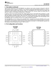
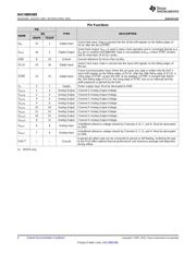
Pin Functions
PIN
TYPE DESCRIPTION
NAME
NO.
WQFN TSSOP
D
IN
15 1 Digital Input
Serial Data Input. Data is clocked into the 16-bit shift register on the falling edges of
SCLK after the fall of SYNC.
D
OUT
16 2 Digital Output
Serial Data Output. D
OUT
is used in daisy chain operation and is connected directly to a
D
IN
pin on another DAC088S085. Data is not available at D
OUT
unless SYNC remains
low for more than 16 SCLK cycles.
GND 8 10 Ground Ground reference for all on-chip circuitry.
SCLK 14 16 Digital Input
Serial Clock Input. Data is clocked into the input shift register on the falling edges of
this pin.
SYNC 13 15 Digital Input
Frame Synchronization Input. When this pin goes low, data is written into the DAC's
input shift register on the falling edges of SCLK. After the 16th falling edge of SCLK, a
rising edge of SYNC causes the DAC to be updated. If SYNC is brought high before
the 15th falling edge of SCLK, the rising edge of SYNC acts as an interrupt and the
write sequence is ignored by the DAC.
V
A
5 7 Supply Power supply input. Must be decoupled to GND.
V
OUTA
1 3 Analog Output Channel A Analog Output Voltage.
V
OUTB
2 4 Analog Output Channel B Analog Output Voltage.
V
OUTC
3 5 Analog Output Channel C Analog Output Voltage.
V
OUTD
4 6 Analog Output Channel D Analog Output Voltage.
V
OUTE
12 14 Analog Output Channel E Analog Output Voltage.
V
OUTF
11 13 Analog Output Channel F Analog Output Voltage.
V
OUTG
10 12 Analog Output Channel G Analog Output Voltage.
V
OUTH
9 11 Analog Output Channel H Analog Output Voltage.
V
REF1
6 8 Analog Input
Unbuffered reference voltage shared by Channels A, B, C, and D. Must be decoupled
to GND.
V
REF2
7 9 Analog Input
Unbuffered reference voltage shared by Channels E, F, G, and H. Must be decoupled
to GND.
PAD
(1)
— — Ground
Exposed die attach pad can be connected to ground or left floating. Soldering the pad
to the PCB offers optimal thermal performance and enhances package self-alignment
during reflow.
器件 Datasheet 文档搜索
AiEMA 数据库涵盖高达 72,405,303 个元件的数据手册,每天更新 5,000 多个 PDF 文件
