Datasheet 搜索 > DA转换器 > National Semiconductor(美国国家半导体) > DAC088S085CISQ 数据手册 > DAC088S085CISQ 数据手册 6/37 页
 器件3D模型
¥ 2.759
DAC088S085CISQ 数据手册 - National Semiconductor(美国国家半导体)
制造商:
National Semiconductor(美国国家半导体)
分类:
DA转换器
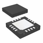
封装:
WFQFN-16
描述:
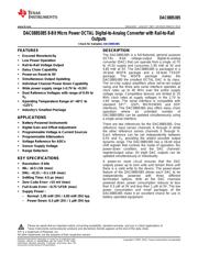
8位微功耗八路数字 - 模拟转换器具有轨至轨输出 8-Bit Micro Power OCTAL Digital-to-Analog Converter with Rail-to-Rail Outputs
Pictures:
3D模型
符号图
焊盘图
引脚图
产品图
页面导航:
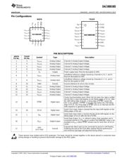
引脚图在P3Hot
典型应用电路图在P23
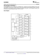
原理图在P2P16
封装尺寸在P29P31P32P34
焊盘布局在P35
标记信息在P29
封装信息在P29P30P31P32
焊接温度在P5
功能描述在P15
技术参数、封装参数在P1P4
应用领域在P1P19P37
电气规格在P4P5P6P7P9P11P12P13P14P16
导航目录
DAC088S085CISQ数据手册
Page:
of 37 Go
若手册格式错乱,请下载阅览PDF原文件
DAC088S085
SNAS424C –AUGUST 2007–REVISED MARCH 2013
www.ti.com
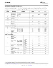
Electrical Characteristics (continued)
The following specifications apply for V
A
= +2.7V to +5.5V, V
REF1
= V
REF2
= V
A
, C
L
= 200 pF to GND, f
SCLK
= 30 MHz, input
code range 3 to 252. Boldface limits apply for T
MIN
≤ T
A
≤ T
MAX
and all other limits are at T
A
= 25°C, unless otherwise
specified.
Limits Units
Symbol Parameter Conditions Typical
(1)
(Limits)
Continuous T
A
= 105°C 10 mA (max)
I
O
Output Current
T
A
= 125°C 6.5 mA (max)
per channel
(2)
R
L
= ∞ 1500 pF
Maximum Load
C
L
Capacitance
R
L
= 2kΩ 1500 pF
DC Output
Z
OUT
8 Ω
Impedance
REFERENCE INPUT CHARACTERISTICS
Input Range
0.5 2.7 V (min)
Minimum
VREF1,2 Input Range
V
A
V (max)
Maximum
Input Impedance 30 kΩ
LOGIC INPUT CHARACTERISTICS
I
IN
Input Current
(2)
±1 µA (max)
V
A
= 2.7V to 3.6V 1.0 0.6 V (max)
V
IL
Input Low Voltage
V
A
= 4.5V to 5.5V 1.1 0.8 V (max)
V
A
= 2.7V to 3.6V 1.4 2.1 V (min)
Input High
V
IH
Voltage
V
A
= 4.5V to 5.5V 2.0 2.4 V (min)
Input Capacitance
C
IN
3 pF (max)
(4)
POWER REQUIREMENTS
Supply Voltage
2.7 V (min)
Minimum
V
A
Supply Voltage
5.5 V (max)
Maximum
V
A
= 2.7V
460 575 µA (max)
Normal Supply
to 3.6V
f
SCLK
= 30 MHz,
Current for supply
output unloaded
V
A
= 4.5V
pin V
A
650 840 µA (max)
to 5.5V
I
N
V
A
= 2.7V
95 135 µA (max)
Normal Supply
to 3.6V
f
SCLK
= 30 MHz,
Current for V
REF1
output unloaded
V
A
= 4.5V
or V
REF2
160 225 µA (max)
to 5.5V
V
A
= 2.7V
370 µA
Static Supply
to 3.6V
f
SCLK
= 0,
Current for supply
output unloaded
V
A
= 4.5V
pin V
A
440 µA
to 5.5V
I
ST
V
A
= 2.7V
95 µA
Static Supply
to 3.6V
f
SCLK
= 0,
Current for V
REF1
output unloaded
V
A
= 4.5V
or V
REF2
160 µA
to 5.5V
(4) This parameter is specified by design and/or characterization and is not tested in production.
6 Submit Documentation Feedback Copyright © 2007–2013, Texas Instruments Incorporated
Product Folder Links: DAC088S085
器件 Datasheet 文档搜索
AiEMA 数据库涵盖高达 72,405,303 个元件的数据手册,每天更新 5,000 多个 PDF 文件
