Datasheet 搜索 > National Semiconductor(美国国家半导体) > DAC088S085EB 数据手册 > DAC088S085EB 数据手册 3/24 页


¥ 0
DAC088S085EB 数据手册 - National Semiconductor(美国国家半导体)
制造商:
National Semiconductor(美国国家半导体)
描述:
8位微功耗八路数字 - 模拟转换器具有轨至轨输出 8-Bit Micro Power OCTAL Digital-to-Analog Converter with Rail-to-Rail Outputs
Pictures:
3D模型
符号图
焊盘图
引脚图
产品图
DAC088S085EB数据手册
Page:
of 24 Go
若手册格式错乱,请下载阅览PDF原文件
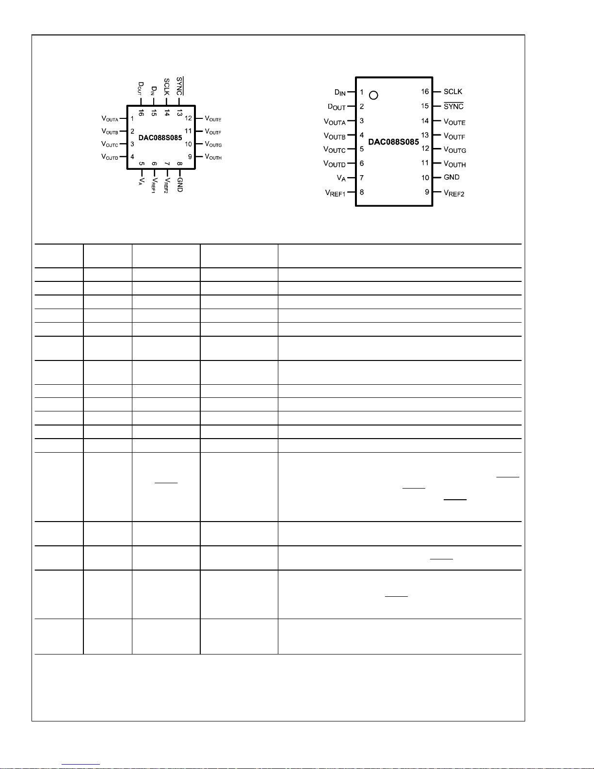
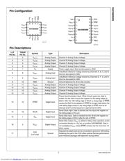
Pin Configuration
30031301
30031302
Pin Descriptions
LLP
Pin No.
TSSOP
Pin No.
Symbol Type Description
1 3
V
OUTA
Analog Output Channel A Analog Output Voltage.
2 4
V
OUTB
Analog Output Channel B Analog Output Voltage.
3 5
V
OUTC
Analog Output Channel C Analog Output Voltage.
4 6
V
OUTD
Analog Output Channel D Analog Output Voltage.
5 7
V
A
Supply Power supply input. Must be decoupled to GND.
6 8
V
REF1
Analog Input
Unbuffered reference voltage shared by Channels A, B, C, and D.
Must be decoupled to GND.
7 9
V
REF2
Analog Input
Unbuffered reference voltage shared by Channels E, F, G, and H.
Must be decoupled to GND.
8 10 GND Ground Ground reference for all on-chip circuitry.
9 11
V
OUTH
Analog Output Channel H Analog Output Voltage.
10 12
V
OUTG
Analog Output Channel G Analog Output Voltage.
11 13
V
OUTF
Analog Output Channel F Analog Output Voltage.
12 14
V
OUTE
Analog Output Channel E Analog Output Voltage.
13 15 SYNC Digital Input
Frame Synchronization Input. When this pin goes low, data is
written into the DAC's input shift register on the falling edges of
SCLK. After the 16th falling edge of SCLK, a rising edge of SYNC
causes the DAC to be updated. If SYNC is brought high before the
15th falling edge of SCLK, the rising edge of SYNC acts as an
interrupt and the write sequence is ignored by the DAC.
14 16 SCLK Digital Input
Serial Clock Input. Data is clocked into the input shift register on
the falling edges of this pin.
15 1
D
IN
Digital Input
Serial Data Input. Data is clocked into the 16-bit shift register on
the falling edges of SCLK after the fall of SYNC.
16 2
D
OUT
Digital Output
Serial Data Output. D
OUT
is utilized in daisy chain operation and is
connected directly to a D
IN
pin on another DAC088S085. Data is
not available at D
OUT
unless SYNC remains low for more than 16
SCLK cycles.
17
PAD
(LLP only)
Ground
Exposed die attach pad can be connected to ground or left floating.
Soldering the pad to the PCB offers optimal thermal performance
and enhances package self-alignment during reflow.
3 www.national.com
DAC088S085
Downloaded from Elcodis.com electronic components distributor
器件 Datasheet 文档搜索
AiEMA 数据库涵盖高达 72,405,303 个元件的数据手册,每天更新 5,000 多个 PDF 文件
