Datasheet 搜索 > TI(德州仪器) > DAC1282 数据手册 > DAC1282 数据手册 1/43 页
 器件3D模型
¥ 0
DAC1282 数据手册 - TI(德州仪器)
制造商:
TI(德州仪器)
封装:
TSSOP-24
描述:
DAC1282 产品数据表
Pictures:
3D模型
符号图
焊盘图
引脚图
产品图
页面导航:
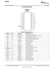
引脚图在P6P21Hot
原理图在P13P14
封装尺寸在P38P39P40
型号编码规则在P2
封装信息在P2P38P39P40
功能描述在P6
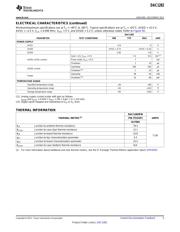
技术参数、封装参数在P2P25
应用领域在P1P43
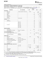
电气规格在P3P4P5P25
型号编号列表在P25
导航目录
DAC1282数据手册
Page:
of 43 Go
若手册格式错乱,请下载阅览PDF原文件
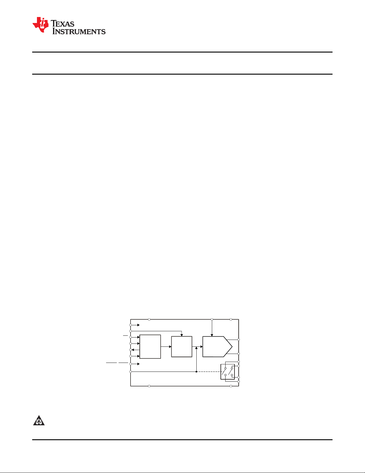
Digital
Signal
Generator
Serial
Interface
VREFDVDD AVDD
DGND AVSS
CLK
SW/TD
SYNC
CS
DIN
DOUT
SCLK
PWDNRESET/
DAC1282
Voltage
Output
DAC
VOUTN
VOUTP
Switch In
Optional Bitstream Input
Switch Out
DAC1282
www.ti.com
SBAS490 –DECEMBER 2011
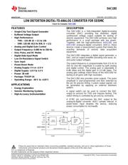
LOW DISTORTION DIGITAL-TO-ANALOG CONVERTER FOR SEISMIC
Check for Samples: DAC1282
1
FEATURES
DESCRIPTION
The DAC1282 is a fully-integrated digital-to-analog
23
• Single-Chip Test Signal Generator
converter (DAC) providing low distortion, digital
• Buffered Voltage Output
synthesized voltage output suitable for testing of
• High Performance:
seismic equipment. The DAC1282 achieves very high
performance in a small package with low power.
– THD: –125 dB (G = 1/1 to 1/8)
Together, with the high-performance ADS1281 and
– SNR: 120 dB (413 Hz BW, G = 1/1)
ADS1282 analog-to-digital converters (ADCs), these
• Analog and Digital Gain Control
devices create a measurement system that meets the
exacting demands of seismic data acquisition
• Output Frequency: 0.488 Hz to 250 Hz
equipment.
• Sine, Pulse, and DC Modes
The DAC1282 integrates a digital signal generator, a
• Digital Data Input Mode
DAC, and an output amplifier providing sine wave, dc,
• Low On-Resistance Signal Switch
and pulse output voltages.
• Sync Input
The output frequency is programmable from 0.5 Hz to
• Power-Down Mode
250 Hz and the magnitude is scaled by both analog
• Analog Supply: 5 V or ±2.5 V
and digital control. The analog gain is adjustable in
6-dB steps and the digital gain in 0.5-dB steps. The
• Digital Supply: 1.8 V to 3.3 V
analog gain settings match those of the ADS1282 for
• Power: 38 mW
testing at all gains with high resolution.
• Package: TSSOP-24
The DAC1282 also provides pulse outputs. The pulse
• Operating Range: –50°C to +125°C
amplitude is user-programmed and then selected by
the pin for precise timing. Custom output signals can
APPLICATIONS
be generated by applying an external bitstream
pattern.
• Energy Exploration
• Seismic Monitoring Systems
A signal switch can be used to connect the DAC
output to sensors for THD and impulse testing. The
• High-Accuracy Instrumentation
switch timing is controlled by pin and by command.
A SYNC pin synchronizes the DAC output to the
analog-to-digital converter (ADC) sample interval. A
power-down input disables the device, reducing
power consumption to microwatts.
1
Please be aware that an important notice concerning availability, standard warranty, and use in critical applications of Texas
Instruments semiconductor products and disclaimers thereto appears at the end of this data sheet.
2SPI is a trademark of Motorola.
3All other trademarks are the property of their respective owners.
PRODUCTION DATA information is current as of publication date.
Copyright © 2011, Texas Instruments Incorporated
Products conform to specifications per the terms of the Texas
Instruments standard warranty. Production processing does not
necessarily include testing of all parameters.
器件 Datasheet 文档搜索
AiEMA 数据库涵盖高达 72,405,303 个元件的数据手册,每天更新 5,000 多个 PDF 文件
