Datasheet 搜索 > DA转换器 > TI(德州仪器) > DAC128S085CISQX 数据手册 > DAC128S085CISQX 数据手册 1/35 页
 器件3D模型
¥ 0
DAC128S085CISQX 数据手册 - TI(德州仪器)
制造商:
TI(德州仪器)
分类:
DA转换器
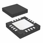
封装:
WFQFN-16
描述:
数模转换器- DAC 12-Bit Micro Power OCTAL Digital-to-Analog Converter with Rail-to-Rail Outputs 16-WQFN -40 to 125
Pictures:
3D模型
符号图
焊盘图
引脚图
产品图
页面导航:
引脚图在P4Hot
典型应用电路图在P22P23
原理图在P1P15P16
封装尺寸在P27P29P30P32
焊盘布局在P33
标记信息在P27
封装信息在P26P27P28P29P30
技术参数、封装参数在P5
应用领域在P1P35
电气规格在P5P6P7P8P9P17

导航目录
DAC128S085CISQX数据手册
Page:
of 35 Go
若手册格式错乱,请下载阅览PDF原文件
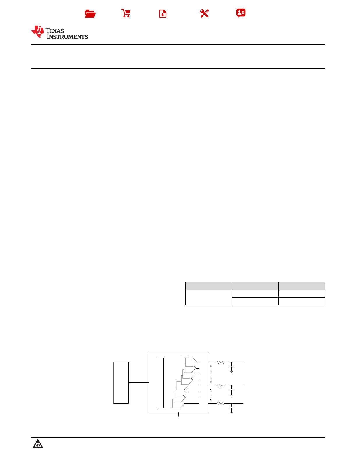
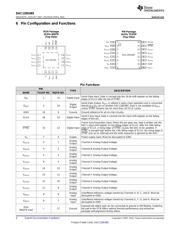
OUTA
OUTB
OUTC
OUTD
OUTE
OUTF
OUTG
OUTH
GND
4-wire SPI
MCU
(Master)
CONTROLLER
VREF1VREF2VDD
2 Individual
References
independent of
VDD
Digital I/O
tolerant of
Master to DAC
rail potential
mismatch
Wide supply range
Product
Folder
Sample &
Buy
Technical
Documents
Tools &
Software
Support &
Community
DAC128S085
SNAS407H –AUGUST 2007–REVISED APRIL 2015
DAC128S085 12-Bit Micro-Power OCTAL Digital-to-Analog Converter With Rail-to-Rail
Outputs
1 Features 3 Description
The DAC128S085 is a full-featured, general-purpose
1
• Ensured Monotonicity
OCTAL 12-bit voltage-output digital-to-analog
• Low Power Operation
converter (DAC) that can operate from a single 2.7-V
• Rail-to-Rail Voltage Output
to 5.5-V supply and consumes 1.95 mW at 3 V and
4.85 mW at 5 V. The DAC128S085 is packaged in a
• Daisy-Chain Capability
16-lead WQFN package and a 16-lead TSSOP
• Power-on Reset to 0 V
package. The WQFN package makes the
• Simultaneous Output Updating
DAC128S085 the smallest OCTAL DAC in its class.
The on-chip output amplifiers allow rail-to-rail output
• Individual Channel Power-Down Capability
swing, and the 3-wire serial interface operates at
• Wide Power Supply Range (2.7 V to 5.5 V)
clock rates up to 40 MHz over the entire supply
• Dual Reference Voltages With Range of 0.5 V to
voltage range. Competitive devices are limited to 25-
V
A
MHz clock rates at supply voltages in the 2.7-V to
• Operating Temperature Range of −40°C to 125°C
3.6-V range. The serial interface is compatible with
standard SPI™, QSPI, MICROWIRE, and DSP
• Smallest Package in the Industry
interfaces. The DAC128S085 also offers daisy-chain
• Resolution 12 Bits
operation, where an unlimited number of
• INL ±8 LSB (Maximum)
DAC128S085s can be updated simultaneously using
a single serial interface.
• DNL 0.75 / −0.4 LSB (Maximum)
• Settling Time 8.5 μs (Maximum)
There are two references for the DAC128S085. One
reference input serves channels A through D, while
• Zero Code Error 15 mV (Maximum)
the other reference serves channels E through H.
• Full-Scale Error −0.75 %FSR (Maximum)
Each reference can be set independently between
• Supply Power
0.5 V and V
A
, providing the widest possible output
dynamic range. The DAC128S085 has a 16-bit input
– 1.95 mW (3 V) / 4.85 mW (5 V) Typical
shift register that controls the mode of operation, the
– Power Down 0.3 μW (3 V) / 1 μW (5 V) Typical
power-down condition, and the register/output value
of the DAC channels. All eight DAC outputs can be
2 Applications
updated simultaneously or individually.
• Battery-Powered Instruments
Device Information
(1)
• Digital Gain and Offset Adjustment
PART NUMBER PACKAGE BODY SIZE (NOM)
• Programmable Voltage and Current Sources
TSSOP (16) 5.00 mm × 4.4 mm
• Programmable Attenuators
DAC128S085
WQFN (16) 4.00 mm × 4.00 mm
• Voltage Reference for ADCs
(1) For all available packages, see the orderable addendum at
• Sensor Supply Voltage
the end of the datasheet.
• Range Detectors
Simplified Schematic
1
An IMPORTANT NOTICE at the end of this data sheet addresses availability, warranty, changes, use in safety-critical applications,
intellectual property matters and other important disclaimers. PRODUCTION DATA.
器件 Datasheet 文档搜索
AiEMA 数据库涵盖高达 72,405,303 个元件的数据手册,每天更新 5,000 多个 PDF 文件
