Datasheet 搜索 > TI(德州仪器) > DAC5687 数据手册 > DAC5687 数据手册 65/79 页

 器件3D模型
¥ 0
DAC5687 数据手册 - TI(德州仪器)
制造商:
TI(德州仪器)
封装:
HTQFP-100
描述:
16 位 500 MSPS 2x-8x 内插双通道数模转换器 (DAC)
Pictures:
3D模型
符号图
焊盘图
引脚图
产品图
页面导航:
引脚图在P33Hot
典型应用电路图在P65
原理图在P2P20P21P22P23P36P39P51P65
封装尺寸在P74P75P76
焊盘布局在P65
型号编码规则在P1
封装信息在P74P75P76
技术参数、封装参数在P5P6P7P8P9P10P20
应用领域在P1P74P79
电气规格在P6P7P8P9P10P20
导航目录
DAC5687数据手册
Page:
of 79 Go
若手册格式错乱,请下载阅览PDF原文件

www.ti.com
Schematic and Layout Recommendations
Application Examples
Application Example: Real IF Radio
DAC5687
SLWS164E – FEBRUARY 2005 – REVISED SEPTEMBER 2006
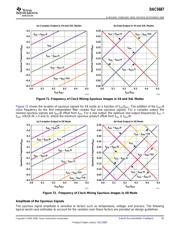
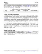
First, the location of the spurious signal is found for the X2 real output in Figure 70 (b). One spurious signal is
present in the range 0 to 0.5 × f
DAC
at 0.325 × f
DAC
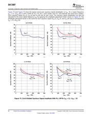
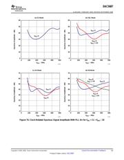
(see Table 17 ). Consulting Figure 74 (a), the raw amplitude for
f
DAC
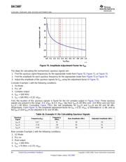
/2 is 47 dBc. From Figure 75 , the amplitude adjustment factor for f
SIG
= 0.175 × f
DAC
is estimated at ~6 dB,
and so the f
DAC
/2 spurious signal is adjusted to 53 dBc.
Table 17. Example # 2 for Calculating Spurious Signals
Spurious Frequency
Frequency/f
DAC
Raw Amplitude (dBc) Adjusted Amplitude (dBc)
Signal (MHz)
f
DAC
/2 0.325 130 47 53
The DAC5687 clock is sensitive to fast transitions of input data on pins DA0, DA1, and DA2 (55, 54, and 53) due
to coupling to DVDD pin 56. The noise-like spectral energy of the DA[2:0] couples into the DAC clock resulting in
increased jitter. This significantly improves by using a 10- Ω resistor between DVDD and pin 56 in addition to
10-pF capacitor to DGND, as implemented on the DAC5687EVM (see the DAC5687 EVM user's guide,
SLWU017) . Pin 56 draws only approximately 2 mA of current and the 0.02-V voltage drop across the resistor is
acceptable for DVDD voltages within the MINIMUM and MAXIMUM specifications. It is also recommended that
the transition rate of the input lines be slowed by inserting series resistors near the data source. The optimized
value of the series resistor depends on the capacitance of the trace between the series resistor and DAC5687
input pin. For a 2 – 3-inch trace, a 22- Ω to 47- Ω resistor is recommended.
The effect of DAC clock jitter on the DAC output signal is worse for signals at higher signal frequencies. For low
IF (< 75 MHz) or baseband signals, there is little degradation of the output signal. However, for high IF (> 75
MHz) the DAC clock jitter may result in an elevated noise floor, which often appears as broad humps in the DAC
output spectrum. It is recommended for signals above 75 MHz that the inputs to DA0 and DA1, which are the two
LSBs if input DA[15:0] is not reversed, not be connected to input data to prevent coupling to the DAC rate clock.
The decrease in resolution to 14 bits and increase in quantization noise does not significantly affect the
DAC5687 SNR for signals > 75 MHz.
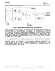
An system example of the DAC5687 used for a flexible real IF radio is shown in Figure 76 . A complex baseband
input to the DAC would be generated by a digital upconverter such as Texas Instruments GC4116, GC5016, or
GC5316. The DAC5687 would be used to increase the data rate through interpolation and flexibly place the
output signal using the FMIX and/or CMIX blocks. Although the DAC5687 X4 mode is shown, any of the modes
(X2, X4L, or X8) would be appropriate.
Copyright © 2005 – 2006, Texas Instruments Incorporated Submit Documentation Feedback 65
Product Folder Link(s): DAC5687
器件 Datasheet 文档搜索
AiEMA 数据库涵盖高达 72,405,303 个元件的数据手册,每天更新 5,000 多个 PDF 文件
