Datasheet 搜索 > DA转换器 > ADI(亚德诺) > DAC8143FS-REEL 数据手册 > DAC8143FS-REEL 数据手册 1/12 页
 器件3D模型
¥ 63.849
DAC8143FS-REEL 数据手册 - ADI(亚德诺)
制造商:
ADI(亚德诺)
分类:
DA转换器
封装:
SOIC
Pictures:
3D模型
符号图
焊盘图
引脚图
产品图
页面导航:
导航目录
DAC8143FS-REEL数据手册
Page:
of 12 Go
若手册格式错乱,请下载阅览PDF原文件
REV. C
Information furnished by Analog Devices is believed to be accurate and
reliable. However, no responsibility is assumed by Analog Devices for its
use, nor for any infringements of patents or other rights of third parties
which may result from its use. No license is granted by implication or
otherwise under any patent or patent rights of Analog Devices.
a
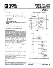
12-Bit Serial Daisy-Chain
CMOS D/A Converter
DAC8143
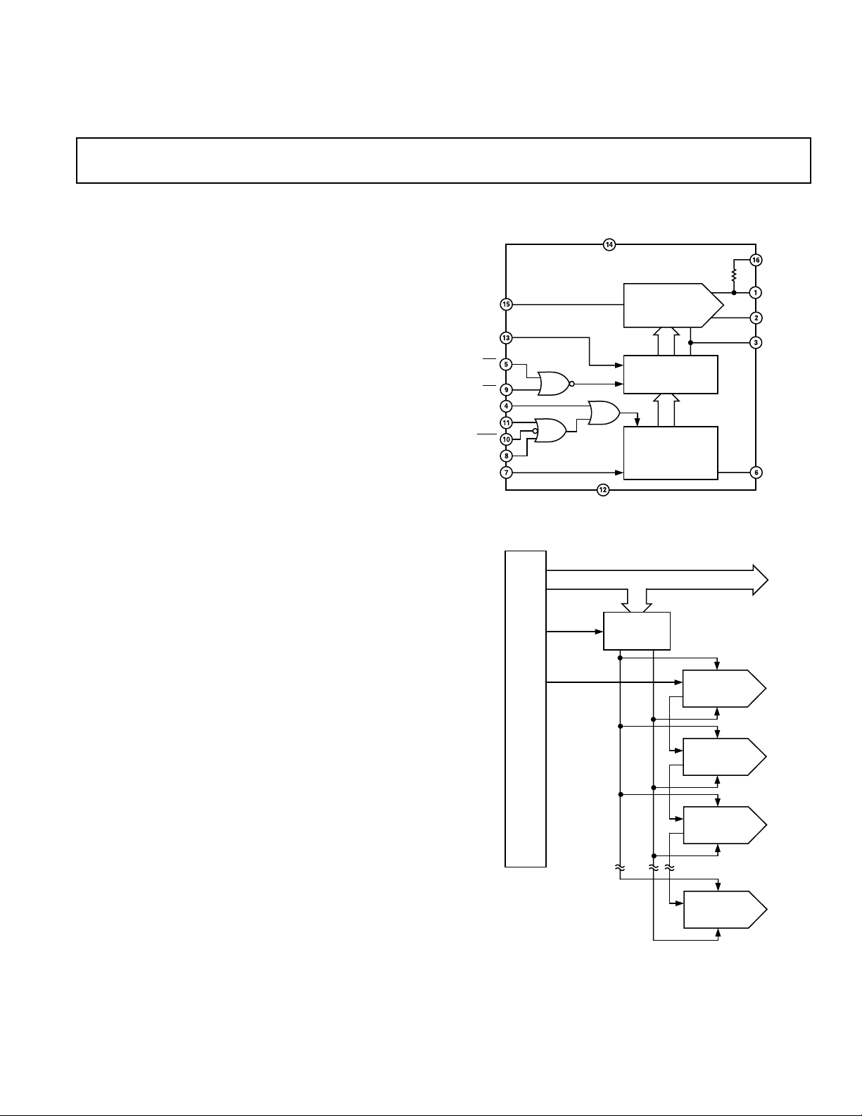
FUNCTIONAL BLOCK DIAGRAM
INPUT 12-BIT
SHIFT REGISTER
DAC REGISTER
12-BIT
D/A CONVERTER
DAC8143
LOAD
IN OUT
CLK
V
DD
R
FB
I
OUT1
I
OUT2
AGND
SRO
DGND
SRI
STB
2
STB
3
STB
4
STB
1
LD
2
LD
1
V
REF
CLR
ADDRESS BUS
ADDRESS
DECODER
STROBE
LOAD
SRI
SRO
DAC8143
STROBE
LOAD
SRI
SRO
DAC8143
STROBE
LOAD
SRI
SRO
DAC8143
STROBE
LOAD
SRI
SRO
DAC8143
WR
DB
X
mP
Figure 1. Multiple DAC8143s with Three-Wire Interface
FEATURES
Fast, Flexible, Microprocessor Interfacing in Serially
Controlled Systems
Buffered Digital Output Pin for Daisy-Chaining
Multiple DACs
Minimizes Address-Decoding in Multiple DAC
Systems—Three-Wire Interface for Any Number of DACs
One Data Line
One CLK Line
One Load Line
Improved Resistance to ESD
–40ⴗC to +85ⴗC for the Extended Industrial Temperature
Range
APPLICATIONS
Multiple-Channel Data Acquisition Systems
Process Control and Industrial Automation
Test Equipment
Remote Microprocessor-Controlled Systems
GENERAL INFORMATION
The DAC8143 is a 12-bit serial-input daisy-chain CMOS D/A
converter that features serial data input and buffered serial data
output. It was designed for multiple serial DAC systems, where
serially daisy-chaining one DAC after another is greatly simplified.
The DAC8143 also minimizes address decoding lines enabling
simpler logic interfacing. It allows three-wire interface for any
number of DACs: one data line, one CLK line and one load line.
Serial data in the input register (MSB first) is sequentially
clocked out to the SRO pin as the new data word (MSB first) is
simultaneously clocked in from the SRI pin. The strobe inputs
are used to clock in/out data on the rising or falling (user
selected) strobe edges (STB
1
, STB
2
, STB3, STB
4
).
When the shift register’s data has been updated, the new data
word is transferred to the DAC register with use of LD1 and
LD2 inputs.
Separate LOAD control inputs allow simultaneous output up-
dating of multiple DACs. An asynchronous CLEAR input
resets the DAC register without altering data in the input
register.
Improved linearity and gain error performance permits reduced
circuit parts count through the elimination of trimming compo-
nents. Fast interface timing reduces timing design considerations
while minimizing microprocessor wait states.
The DAC8143 is available in plastic packages that are compat-
ible with autoinsertion equipment.
Plastic packaged devices come in the extended industrial tem-
perature range of –40°C to +85°C.
One Technology Way, P.O. Box 9106, Norwood, MA 02062-9106, U.S.A.
Tel: 781/329-4700 World Wide Web Site: http://www.analog.com
Fax: 781/326-8703 © Analog Devices, Inc., 1999
器件 Datasheet 文档搜索
AiEMA 数据库涵盖高达 72,405,303 个元件的数据手册,每天更新 5,000 多个 PDF 文件
