Datasheet 搜索 > Zetex > DMP2240UW-7 数据手册 > DMP2240UW-7 数据手册 1/5 页


¥ 0
DMP2240UW-7 数据手册 - Zetex
制造商:
Zetex
Pictures:
3D模型
符号图
焊盘图
引脚图
产品图
页面导航:
导航目录
DMP2240UW-7数据手册
Page:
of 5 Go
若手册格式错乱,请下载阅览PDF原文件
DMP2240UW
Document number: DS31372 Rev. 3 - 2
1 of 5
www.diodes.com
May 2010
© Diodes Incorporated
DMP2240UW
P-CHANNEL ENHANCEMENT MODE FIELD EFFECT TRANSISTOR
Features
• P-Channel MOSFET
• Low On-Resistance
• 150 mΩ @ V
GS
= -4.5V
• 200 mΩ @ V
GS
= -2.5V
• 240 mΩ @ V
GS
= -1.8V
• Very Low Gate Threshold Voltage V
GS(th)
≤ 1V
• Low Input Capacitance
• Fast Switching Speed
• Low Input/Output Leakage
• Lead Free By Design/RoHS Compliant (Note 2)
• "Green" Device (Note 3)
• Qualified to AEC-Q101 standards for High Reliability
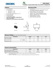
Mechanical Data
• Case: SOT-323
• Case Material: Molded Plastic, “Green” Molding Compound.
UL Flammability Classification Rating 94V-0
• Moisture Sensitivity: Level 1 per J-STD-020
• Terminals Connections: See Diagram Below
• Terminals: Finish ⎯ Matte Tin annealed over Alloy 42
leadframe. Solderable per MIL-STD-202, Method 208
• Marking Information: See Page 4
• Ordering Information: See Page 4
• Weight: 0.006 grams (approximate)
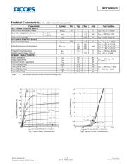
Maximum Ratings @T
A
= 25°C unless otherwise specified
Characteristic Symbol Value Units
Drain-Source Voltage
V
DSS
-20 V
Gate-Source Voltage
V
GSS
±12 V
Drain Current (Note 1)
T
A
= 25°C
T
A
= 70°C
I
D
-1.5
-1.0
A
Pulsed Drain Current
I
DM
-5 A
Thermal Characteristics
Characteristic Symbol Value Units
Total Power Dissipation (Note 1)
P
D
250 mW
Thermal Resistance, Junction to Ambient
R
θ
JA
500 °C/W
Operating and Storage Temperature Range
T
J,
T
STG
-55 to +150 °C
Notes: 1. Device mounted on FR-4 substrate PC board, 2oz. Copper, with minimum recommended pad layout.
2. No purposefully added lead.
3. Diodes Inc.’s “Green” policy can be found on our website at http://www.diodes.com/products/lead_free/index.php.
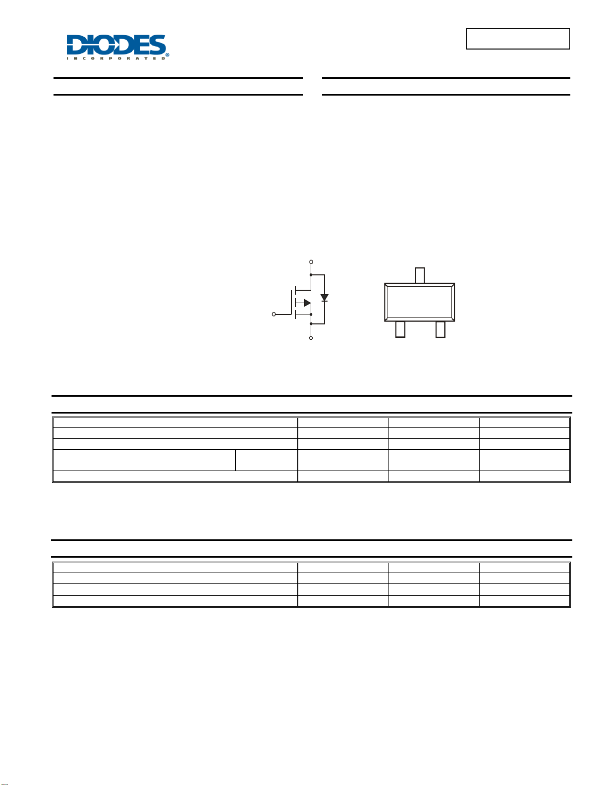
SOT-323
Top View
To
p
View
Internal Schematic
Source
Gate
Drain
GS
D
器件 Datasheet 文档搜索
AiEMA 数据库涵盖高达 72,405,303 个元件的数据手册,每天更新 5,000 多个 PDF 文件
