Datasheet 搜索 > Supertex(超科) > DN2540N5 数据手册 > DN2540N5 数据手册 1/4 页

¥ 0
DN2540N5 数据手册 - Supertex(超科)
制造商:
Supertex(超科)
封装:
TO-220
Pictures:
3D模型
符号图
焊盘图
引脚图
产品图
页面导航:
导航目录
DN2540N5数据手册
Page:
of 4 Go
若手册格式错乱,请下载阅览PDF原文件
1
12/13/01
Supertex Inc. does not recommend the use of its products in life support applications and will not knowingly sell its products for use in such applications unless it receives an adequate "products liability
indemnification insurance agreement." Supertex does not assume responsibility for use of devices described and limits its liability to the replacement of devices determined to be defective due to
workmanship. No responsibility is assumed for possible omissions or inaccuracies. Circuitry and specifications are subject to change without notice. For the latest product specifications, refer to the
Supertex website: http://www.supertex.com. For complete liability information on all Supertex products, refer to the most current databook or to the Legal/Disclaimer page on the Supertex website.
DN2535
DN2540
Advanced DMOS Technology
Not recommended for new designs. For products in TO-92
(N3) package and TO-243AA (N8) package, please use DN3535
or DN3545 instead.
These low threshold depletion-mode (normally-on) transistors
utilize an advanced vertical DMOS structure and Supertex’s
well-proven silicon-gate manufacturing process. This combina-
tion produces devices with the power handling capabilities of
bipolar transistors and with the high input impedance and posi-
tive temperature coefficient inherent in MOS devices. Character-
istic of all MOS structures, these devices are free from thermal
runaway and thermally-induced secondary breakdown.
Supertex’s vertical DMOS FETs are ideally suited to a wide range
of switching and amplifying applications where high breakdown
voltage, high input impedance, low input capacitance, and fast
switching speeds are desired.
Features
❏ High input impedance
❏ Low input capacitance
❏ Fast switching speeds
❏ Low on resistance
❏ Free from secondary breakdown
❏ Low input and output leakage
Applications
❏ Normally-on switches
❏ Solid state relays
❏ Converters
❏ Linear amplifiers
❏ Constant current sources
❏ Power supply circuits
❏ Telecom
Absolute Maximum Ratings
Drain-to-Source Voltage BV
DSX
Drain-to-Gate Voltage BV
DGX
Gate-to-Source Voltage ± 20V
Operating and Storage Temperature -55°C to +150°C
Soldering Temperature* 300°C
*
Distance of 1.6 mm from case for 10 seconds.
Note: See Package Outline section for dimensions.
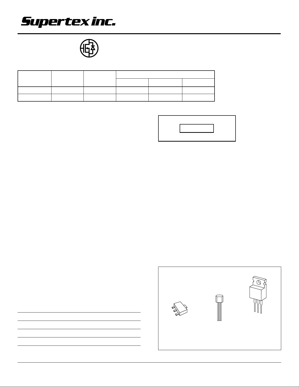
Package Options
N-Channel Depletion-Mode
Vertical DMOS FETs
TO-92
S G D
TO-243AA
(SOT-89)
G
D
S
D
TO-220
TAB: DRAIN
G
D
S
Product marking for TO-243AA:
DN5D❋
Where ❋ = 2-week alpha date code
* Same as SOT-89. Product shipped on 2000 piece carrier tape reels.
BV
DSX
/R
DS(ON)
I
DSS
BV
DGX
(max) (min) TO-92 TO-220 TO-243AA*
350V 25Ω 150mA DN2535N3 DN2535N5 —
400V 25Ω 150mA DN2540N3 DN2540N5 DN2540N8
Ordering Information
Order Number / Package
器件 Datasheet 文档搜索
AiEMA 数据库涵盖高达 72,405,303 个元件的数据手册,每天更新 5,000 多个 PDF 文件
