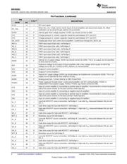
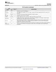
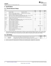
Datasheet 搜索 > 开发套件 > TI(德州仪器) > DRV8301-LS31-KIT 数据手册 > DRV8301-LS31-KIT 数据手册 1/39 页

¥ 3146.909
DRV8301-LS31-KIT 数据手册 - TI(德州仪器)
制造商:
TI(德州仪器)
分类:
开发套件
描述:
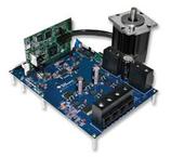
TEXAS INSTRUMENTS DRV8301-LS31-KIT 评估板, 电机控制器, LS31 DRV8301
Pictures:
3D模型
符号图
焊盘图
引脚图
产品图
页面导航:
引脚图在P3P4P5Hot
典型应用电路图在P25P26
原理图在P1P14P16P25P30
封装尺寸在P32P34P35
标记信息在P32
封装信息在P31P32P33P34P35
技术参数、封装参数在P6
应用领域在P1P39
电气规格在P8P9
导航目录
DRV8301-LS31-KIT数据手册
Page:
of 39 Go
若手册格式错乱,请下载阅览PDF原文件
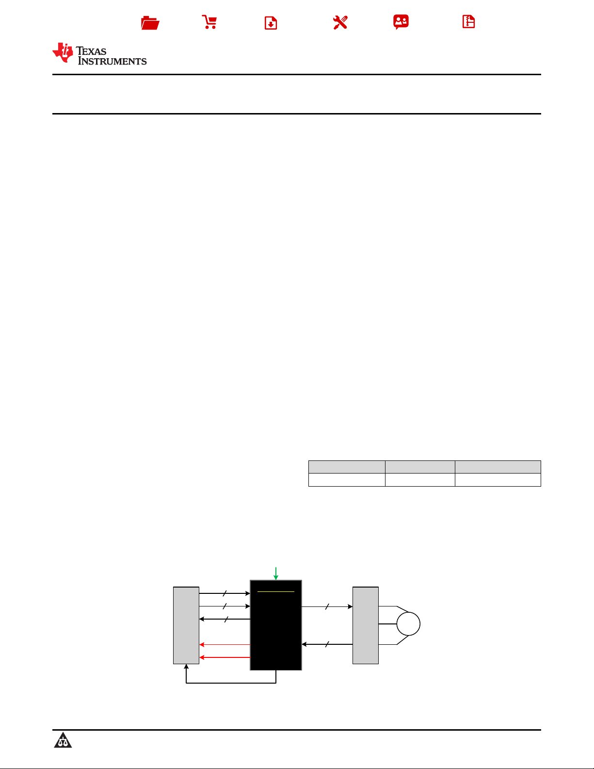
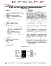
DRV8301
PWM
6 to 60 V
MCU
N-Channel
MOSFETs
Gate Drive
Sense
3-Phase
Brushless
Pre-Driver
Buck
Converter
SPI
nFAULT
nOCTW
Vcc (Buck)
Diff Amps
M
Product
Folder
Sample &
Buy
Technical
Documents
Tools &
Software
Support &
Community
Reference
Design
An IMPORTANT NOTICE at the end of this data sheet addresses availability, warranty, changes, use in safety-critical applications,
intellectual property matters and other important disclaimers. PRODUCTION DATA.
DRV8301
SLOS719F –AUGUST 2011–REVISED JANUARY 2016
DRV8301 Three-Phase Gate Driver With Dual Current Shunt Amplifiers
and Buck Regulator
1
1 Features
1
• 6-V to 60-V Operating Supply Voltage Range
• 1.7-A Source and 2.3-A Sink Gate Drive Current
Capability
• Slew Rate Control for EMI Reduction
• Bootstrap Gate Driver With 100% Duty Cycle
Support
• 6- or 3-PWM Input Modes
• Dual Integrated Current Shunt Amplifiers With
Adjustable Gain and Offset
• Integrated 1.5-A Buck Converter
• 3.3-V and 5-V Interface Support
• SPI
• Protection Features:
– Programmable Dead Time Control (DTC)
– Programmable Overcurrent Protection (OCP)
– PVDD and GVDD Undervoltage Lockout
(UVLO)
– GVDD Overvoltage Lockout (OVLO)
– Overtemperature Warning/Shutdown
(OTW/OTS)
– Reported Through nFAULT, nOCTW, and SPI
Registers
2 Applications
• 3-Phase BLDC and PMSM Motors
• CPAPs and Pumps
• E-bikes
• Power Tools
• Robotics and RC Toys
• Industrial Automation
3 Description
The DRV8301 is a gate driver IC for three-phase
motor drive applications. The device provides three
half-bridge drivers, each capable of driving two N-
channel MOSFETs. The DRV8301 supports up to
1.7-A source and 2.3-A peak current capability. The
DRV8301 can operate off of a single power supply
with a wide range from 6-V to 60-V. The device uses
a bootstrap gate driver architecture with trickle charge
circuitry to support 100% duty cycle. The DRV8301
uses automatic handshaking when the high-side or
low-side MOSFET is switching to prevent flow of
current. Integrated VDS sensing of the high-side and
low-side MOSFETs is used to protect the external
power stage against overcurrent conditions.
The DRV8301 includes two current shunt amplifiers
for accurate current measurement. The amplifiers
support bidirectional current sensing and provide an
adjustable output offset up to 3 V.
The DRV8301 also includes an integrated switching
mode buck converter with adjustable output and
switching frequency. The buck converter can provide
up to 1.5 A to support MCU or additional system
power needs.
The SPI provides detailed fault reporting and flexible
parameter settings such as gain options for the
current shunt amplifiers and slew rate control of the
gate drivers.
Device Information
(1)
PART NUMBER PACKAGE BODY SIZE (NOM)
DRV8301 HTSSOP (56) 14.00 mm × 8.10 mm
(1) For all available packages, see the orderable addendum at
the end of the data sheet.
Simplified Schematic
器件 Datasheet 文档搜索
AiEMA 数据库涵盖高达 72,405,303 个元件的数据手册,每天更新 5,000 多个 PDF 文件
