Datasheet 搜索 > 电机驱动器 > TI(德州仪器) > DRV8332DKD 数据手册 > DRV8332DKD 数据手册 2/39 页


¥ 79.402
DRV8332DKD 数据手册 - TI(德州仪器)
制造商:
TI(德州仪器)
分类:
电机驱动器
封装:
BSSOP-36
描述:
TEXAS INSTRUMENTS DRV8332DKD 芯片, 电机驱动器, PWM, 三相, 36HSSOP
Pictures:
3D模型
符号图
焊盘图
引脚图
产品图
页面导航:
引脚图在P4P5Hot
典型应用电路图在P16
原理图在P10P16P19P20P21P22P26
封装尺寸在P30P32P33
焊盘布局在P28
标记信息在P30
封装信息在P29P30P31P32P33
技术参数、封装参数在P6P8
应用领域在P1P16P39
电气规格在P8P11P23P24
导航目录
DRV8332DKD数据手册
Page:
of 39 Go
若手册格式错乱,请下载阅览PDF原文件
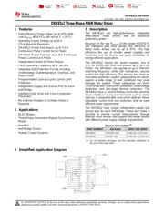
DRV8312
,
DRV8332
SLES256E –MAY 2010–REVISED DECEMBER 2014
www.ti.com
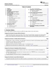
Table of Contents
8.4 Device Functional Modes........................................ 14
1 Features.................................................................. 1
9 Application and Implementation ........................ 16
2 Applications ........................................................... 1
9.1 Application Information............................................ 16
3 Description ............................................................. 1
9.2 Typical Applications ................................................ 16
4 Simplified Application Diagram............................ 1
10 Power Supply Recommendations ..................... 23
5 Revision History..................................................... 2
10.1 Bulk Capacitance.................................................. 23
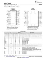
6 Pin Configuration and Functions......................... 4
10.2 System Power-Up and Power-Down Sequence... 23
7 Specifications......................................................... 6
10.3 System Design Recommendations....................... 24
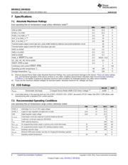
7.1 Absolute Maximum Ratings...................................... 6
11 Layout................................................................... 25
7.2 ESD Ratings.............................................................. 6
11.1 Layout Guidelines ................................................. 25
7.3 Recommended Operating Conditions....................... 6
11.2 Layout Example .................................................... 25
7.4 Thermal Information.................................................. 7
11.3 Thermal Considerations........................................ 28
7.5 Dissipation Ratings ................................................... 7
12 Device and Documentation Support................. 29
7.6 Power Deratings (DRV8312) .................................... 7
12.1 Related Links ........................................................ 29
7.7 Electrical Characteristics........................................... 8
12.2 Trademarks........................................................... 29
7.8 Typical Characteristics.............................................. 9
12.3 Electrostatic Discharge Caution............................ 29
8 Detailed Description............................................ 10
12.4 Glossary................................................................ 29
8.1 Overview................................................................. 10
13 Mechanical, Packaging, and Orderable
8.2 Functional Block Diagram....................................... 10
Information........................................................... 29
8.3 Feature Description................................................. 10
5 Revision History
NOTE: Page numbers for previous revisions may differ from page numbers in the current version.
Changes from Revision D (January 2014) to Revision E Page
• Added ESD Ratings table, Features Description section, Device Functional Modes, Application and Implementation
section, Power Supply Recommendations section, Layout section, Device and Documentation Support section................ 1
Changes from Revision C (October 2013) to Revision D Page
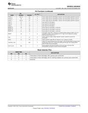
• Changed GND_A, GND_B, and GND_C pins description to remove text "requires close decoupling capacitor to ground". 4
• Changed M2 pin description From: Mode selection pin......................................................................................................... 4
• Added the THERMAL INFORMATION table.......................................................................................................................... 7
• Added text to the Overcurrent (OC) Protection section - "It is important to note..." ............................................................ 12
• Added text to the Overcurrent (OC) Protection section - "The values in Table 2 show typical..." ...................................... 12
Changes from Revision B (September 2013) to Revision C Page
• Changed text in the Overcurrent (OC) Protection section From: "cause the device to shutdown immediately." To:
"cause the device to shutdown."........................................................................................................................................... 12
• Changed Changed text in the Overcurrent (OC) Protection section From: "RESET_B, and / or must be asserted."
To: ", and must be asserted"................................................................................................................................................ 12
• Changed paragraph in the DEVICE RESET "A rising-edge transition..."............................................................................. 13
Changes from Revision A (July 2013) to Revision B Page
• Changed the description of pin M3 From: AGND connection is recommended To: VREG connection is recommended..... 4
2 Submit Documentation Feedback Copyright © 2010–2014, Texas Instruments Incorporated
Product Folder Links: DRV8312 DRV8332
器件 Datasheet 文档搜索
AiEMA 数据库涵盖高达 72,405,303 个元件的数据手册,每天更新 5,000 多个 PDF 文件
