Datasheet 搜索 > 接口芯片 > TI(德州仪器) > DS90LV031ATMX 数据手册 > DS90LV031ATMX 数据手册 5/19 页
 器件3D模型
¥ 14.645
DS90LV031ATMX 数据手册 - TI(德州仪器)
制造商:
TI(德州仪器)
分类:
接口芯片
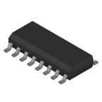
封装:
SOIC-16
描述:
DS90LV031A 3V LVDS四通道CMOS差分线路驱动器 DS90LV031A 3V LVDS Quad CMOS Differential Line Driver
Pictures:
3D模型
符号图
焊盘图
引脚图
产品图
页面导航:
导航目录
DS90LV031ATMX数据手册
Page:
of 19 Go
若手册格式错乱,请下载阅览PDF原文件
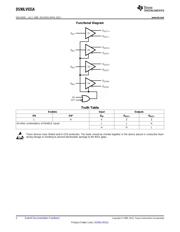
DS90LV031A
www.ti.com
SNLS020C –JULY 1999–REVISED APRIL 2013
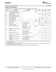
Switching Characteristics - Industrial
V
CC
= +3.3V ±10%, T
A
= −40°C to +85°C
(1) (2) (3)
Symbol Parameter Conditions Min Typ Max Units
t
PHLD
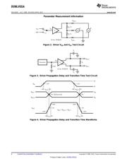
Differential Propagation Delay High to Low R
L
= 100Ω, C
L
= 10 pF 0.8 1.18 2.0 ns
(Figure 3 and Figure 4)
t
PLHD
Differential Propagation Delay Low to High 0.8 1.25 2.0 ns
t
SKD1
Differential Pulse Skew |t
PHLD
− t
PLHD
|
(4)
0 0.07 0.4 ns
t
SKD2
Channel-to-Channel Skew
(5)
0 0.1 0.5 ns
t
SKD3
Differential Part to Part Skew
(6)
0 1.0 ns
t
SKD4
Differential Part to Part Skew
(7)
0 1.2 ns
t
TLH
Rise Time 0.38 1.5 ns
t
THL
Fall Time 0.40 1.5 ns
t
PHZ
Disable Time High to Z R
L
= 100Ω, C
L
= 10 pF 5 ns
(Figure 5 and Figure 6)
t
PLZ
Disable Time Low to Z 5 ns
t
PZH
Enable Time Z to High 7 ns
t
PZL
Enable Time Z to Low 7 ns
f
MAX
Maximum Operating Frequency
(8)
200 250 MHz
(1) All typicals are given for: V
CC
= +3.3V, T
A
= +25°C.
(2) Generator waveform for all tests unless otherwise specified: f = 1 MHz, Z
O
= 50Ω, t
r
≤ 1 ns, and t
f
≤ 1 ns.
(3) C
L
includes probe and jig capacitance.
(4) t
SKD1
, |t
PHLD
− t
PLHD
| is the magnitude difference in differential propagation delay time between the positive going edge and the negative
going edge of the same channel.
(5) t
SKD2
is the Differential Channel-to-Channel Skew of any event on the same device.
(6) t
SKD3
, Differential Part to Part Skew, is defined as the difference between the minimum and maximum specified differential propagation
delays. This specification applies to devices at the same V
CC
and within 5°C of each other within the operating temperature range.
(7) t
SKD4
, part to part skew, is the differential channel-to-channel skew of any event between devices. This specification applies to devices
over recommended operating temperature and voltage ranges, and across process distribution. t
SKD4
is defined as |Max − Min|
differential propagation delay.
(8) f
MAX
generator input conditions: t
r
= t
f
< 1ns, (0% to 100%), 50% duty cycle, 0V to 3V. Output Criteria: duty cycle = 45%/55%, VOD >
250mV, all channels switching.
Copyright © 1999–2013, Texas Instruments Incorporated Submit Documentation Feedback 5
Product Folder Links: DS90LV031A
器件 Datasheet 文档搜索
AiEMA 数据库涵盖高达 72,405,303 个元件的数据手册,每天更新 5,000 多个 PDF 文件
