Datasheet 搜索 > TI(德州仪器) > DS90UB947TRGCRQ1 数据手册 > DS90UB947TRGCRQ1 数据手册 70/81 页
 器件3D模型
¥ 28.321
DS90UB947TRGCRQ1 数据手册 - TI(德州仪器)
制造商:
TI(德州仪器)
封装:
VQFN-64
描述:
1080p 双路 FPD-Link III 串行器 64-VQFN -40 to 105
Pictures:
3D模型
符号图
焊盘图
引脚图
产品图
页面导航:
引脚图在P3P4P5P70P71Hot
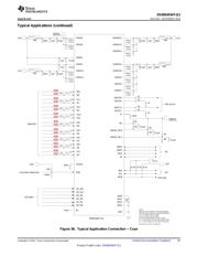
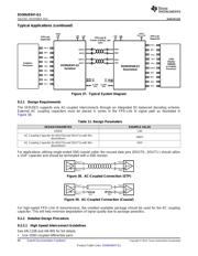
典型应用电路图在P65P66P67P68
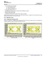
原理图在P14
封装尺寸在P74P76P77
标记信息在P74
封装信息在P73P74P75P76P77
功能描述在P37P38P39P40P41P42P43P44P45P46P47P48
技术参数、封装参数在P6P73
应用领域在P1P65P66P67P68P81
电气规格在P7P8
导航目录
DS90UB947TRGCRQ1数据手册
Page:
of 81 Go
若手册格式错乱,请下载阅览PDF原文件

DS90UB947-Q1
SNLS454 –NOVEMBER 2014
www.ti.com
10 Power Supply Recommendations
This device provides separate power and ground pins for different portions of the circuit. This is done to isolate
switching noise effects between different sections of the circuit. Separate planes on the PCB are typically not
required. The Pin Functions table provides guidance on which circuit blocks are connected to which power pins.
In some cases, an external filter many be used to provide clean power to sensitive circuits such as PLLs.
10.1 Power Up Requirements And PDB Pin
The power supply ramp should be faster than 1.5ms with a monotonic rise. A large capacitor on the PDB pin is
needed to ensure PDB arrives after all the supply pins have settled to the recommended operating voltage.
When PDB pin is pulled up to V
DDIO
, a 10kΩ pull-up and a >10μF capacitor to GND are required to delay the
PDB input signal rise. All inputs must not be driven until all power supplies have reached steady state.
The recommended power up sequence is as follows: V
DD18
, V
DD11
, wait until all supplies have settled, activate
PDB, then apply OpenLDI input.
70 Submit Documentation Feedback Copyright © 2014, Texas Instruments Incorporated
Product Folder Links: DS90UB947-Q1
器件 Datasheet 文档搜索
AiEMA 数据库涵盖高达 72,405,303 个元件的数据手册,每天更新 5,000 多个 PDF 文件
