Datasheet 搜索 > 微控制器 > Microchip(微芯) > DSPIC30F2010-20E/SOG 数据手册 > DSPIC30F2010-20E/SOG 数据手册 53/202 页

 器件3D模型
¥ 34.963
DSPIC30F2010-20E/SOG 数据手册 - Microchip(微芯)
制造商:
Microchip(微芯)
分类:
微控制器
封装:
SOIC
Pictures:
3D模型
符号图
焊盘图
引脚图
产品图
页面导航:
引脚图在P5P95P192Hot
原理图在P8P15P53P58P62P63P67P71P75P82P92P96
标记信息在P185
封装信息在P148P185P190P192P201
功能描述在P91P95
技术参数、封装参数在P117P149P153P154P156P158P180P181P192
电气规格在P57P61P113P117P155P192
导航目录
DSPIC30F2010-20E/SOG数据手册
Page:
of 202 Go
若手册格式错乱,请下载阅览PDF原文件
© 2011 Microchip Technology Inc. DS70118J-page 53
dsPIC30F2010
8.0 I/O PORTS
All of the device pins (except VDD, VSS, MCLR and
OSC1/CLKI) are shared between the peripherals and
the parallel I/O ports.
All I/O input ports feature Schmitt Trigger inputs for
improved noise immunity.
8.1 Parallel I/O (PIO) Ports
When a peripheral is enabled and the peripheral is
actively driving an associated pin, the use of the pin as
a general purpose output pin is disabled. The I/O pin
may be read, but the output driver for the parallel port
bit will be disabled. If a peripheral is enabled, but the
peripheral is not actively driving a pin, that pin may be
driven by a port.
All port pins have three registers directly associated
with the operation of the port pin. The data direction
register (TRISx) determines whether the pin is an input
or an output. If the data direction bit is a ‘1’, then the pin
is an input. All port pins are defined as inputs after a
Reset. Reads from the latch (LATx), read the latch.
Writes to the latch, write the latch (LATx). Reads from
the port (PORTx), read the port pins, and writes to the
port pins, write the latch (LATx).
Any bit and its associated data and control registers
that are not valid for a particular device will be disabled.
That means the corresponding LATx and TRISx
registers and the port pin will read as zeros.
When a pin is shared with another peripheral or func-
tion that is defined as an input only, it is nevertheless
regarded as a dedicated port because there is no
other competing source of outputs. An example is the
INT4 pin.
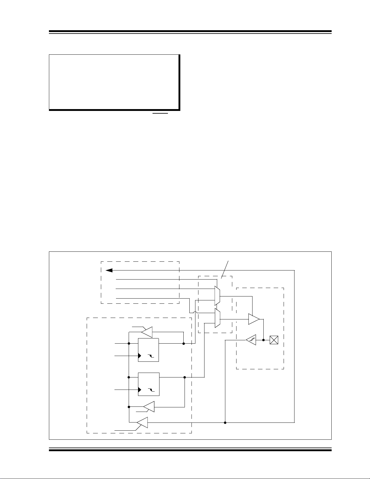
A parallel I/O (PIO) port that shares a pin with a periph-
eral is, in general, subservient to the peripheral. The
peripheral’s output buffer data and control signals are
provided to a pair of multiplexers. The multiplexers
select whether the peripheral or the associated port
has ownership of the output data and control signals of
the I/O pad cell. Figure 8-1 shows how ports are shared
with other peripherals, and the associated I/O cell (pad)
to which they are connected. Table 8-1 shows the
formats of the registers for the shared ports, PORTB
through PORTF.
FIGURE 8-1: BLOCK DIAGRAM OF A SHARED PORT STRUCTURE
Note: This data sheet summarizes features of
this group of dsPIC30F devices and is not
intended to be a complete reference
source. For more information on the CPU,
peripherals, register descriptions and
general device functionality, refer to the
“dsPIC30F Family Reference Manual”
(DS70046).
Q
D
CK
WR LAT +
TRIS Latch
I/O Pad
WR Port
Data Bus
QD
CK
Data Latch
Read LAT
Read Port
Read TRIS
1
0
1
0
WR TRIS
Peripheral Output Data
Peripheral Input Data
I/O Cell
Peripheral Module
Peripheral Output Enable
PIO Module
Output Multiplexers
Input Data
Peripheral Module Enable
Output Enable
Output Data
器件 Datasheet 文档搜索
AiEMA 数据库涵盖高达 72,405,303 个元件的数据手册,每天更新 5,000 多个 PDF 文件
