Datasheet 搜索 > 微控制器 > Microchip(微芯) > DSPIC30F2010-20E/SOG 数据手册 > DSPIC30F2010-20E/SOG 数据手册 58/202 页

 器件3D模型
¥ 34.963
DSPIC30F2010-20E/SOG 数据手册 - Microchip(微芯)
制造商:
Microchip(微芯)
分类:
微控制器
封装:
SOIC
Pictures:
3D模型
符号图
焊盘图
引脚图
产品图
页面导航:
引脚图在P5P95P192Hot
原理图在P8P15P53P58P62P63P67P71P75P82P92P96
标记信息在P185
封装信息在P148P185P190P192P201
功能描述在P91P95
技术参数、封装参数在P117P149P153P154P156P158P180P181P192
电气规格在P57P61P113P117P155P192
导航目录
DSPIC30F2010-20E/SOG数据手册
Page:
of 202 Go
若手册格式错乱,请下载阅览PDF原文件
dsPIC30F2010
DS70118J-page 58 © 2011 Microchip Technology Inc.
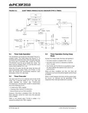
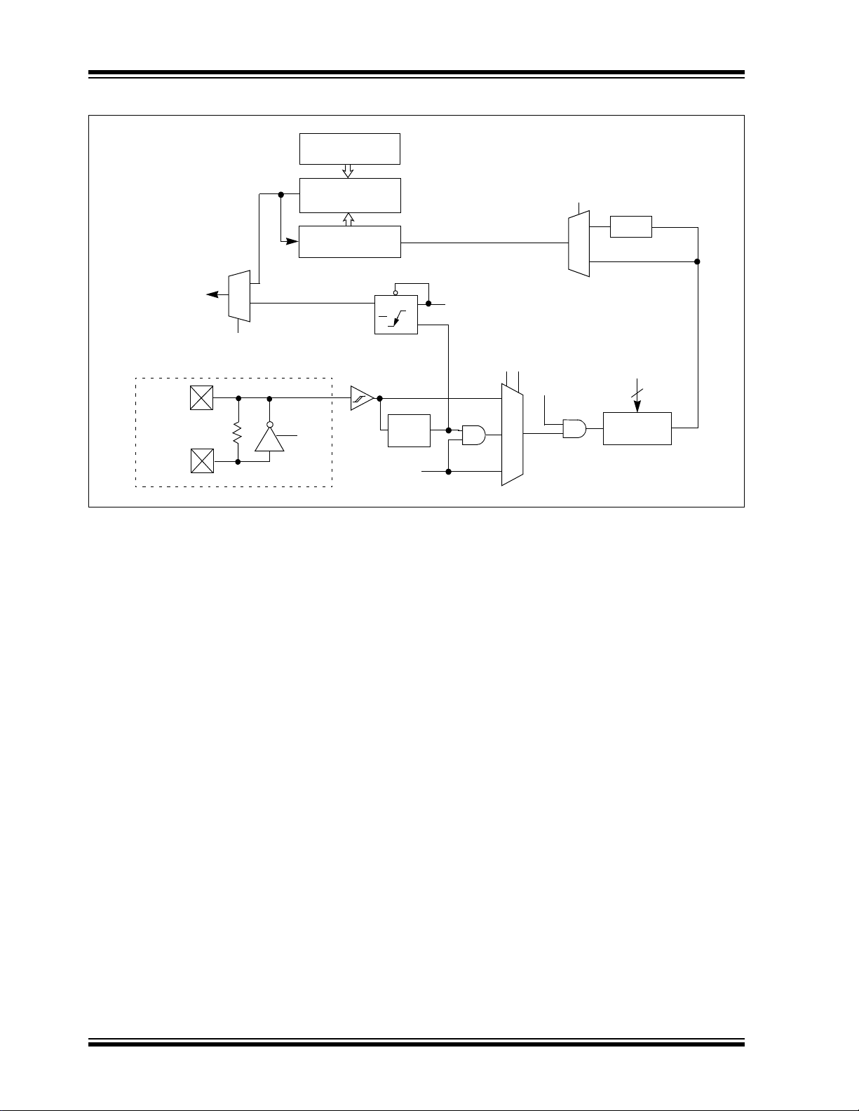
FIGURE 9-1: 16-BIT TIMER1 MODULE BLOCK DIAGRAM (TYPE A TIMER)
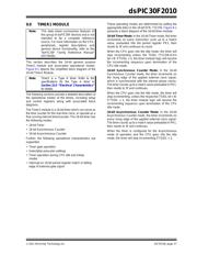
9.1 Timer Gate Operation
The 16-bit timer can be placed in the Gated Time Accu-
mulation mode. This mode allows the internal T
CY to
increment the respective timer when the gate input sig-
nal (T1CK pin) is asserted high. Control bit TGATE
(T1CON<6>) must be set to enable this mode. The
timer must be enabled (TON = 1) and the timer clock
source set to internal (TCS = 0).
When the CPU goes into the Idle mode, the timer will
stop incrementing, unless TSIDL = 0. If TSIDL = 1, the
timer will resume the incrementing sequence upon
termination of the CPU Idle mode.
9.2 Timer Prescaler
The input clock (FOSC/4 or external clock) to the 16-bit
Timer, has a prescale option of 1:1, 1:8, 1:64, and
1:256 selected by control bits TCKPS<1:0>
(T1CON<5:4>). The prescaler counter is cleared when
any of the following occurs:
• A write to the TMR1 register
• Clearing of the TON bit (T1CON<15>)
• Device Reset such as POR and BOR
However, if the timer is disabled (TON = 0), then the
timer prescaler cannot be reset since the prescaler
clock is halted.
TMR1 is not cleared when T1CON is written. It is
cleared by writing to the TMR1 register.
9.3 Timer Operation During Sleep
Mode
During CPU Sleep mode, the timer will operate if:
• The timer module is enabled (TON = 1) and
• The timer clock source is selected as external
(TCS = 1) and
• The TSYNC bit (T1CON<2>) is asserted to a logic
‘0’, which defines the external clock source as
asynchronous
When all three conditions are true, the timer will
continue to count up to the period register and be Reset
to 0x0000.
When a match between the timer and the period regis-
ter occurs, an interrupt can be generated, if the
respective timer interrupt enable bit is asserted.
TON
Sync
SOSCI
SOSCO/
PR1
T1IF
Equal
Comparator x 16
TMR1
Reset
LPOSCEN
Event Flag
1
0
TSYNC
Q
Q
D
CK
TGATE
TCKPS<1:0>
Prescaler
1, 8, 64, 256
2
TGATE
T
CY
1
0
T1CK
TCS
1 X
0 1
TGATE
0 0
(3)
Gate
Sync
器件 Datasheet 文档搜索
AiEMA 数据库涵盖高达 72,405,303 个元件的数据手册,每天更新 5,000 多个 PDF 文件
