Datasheet 搜索 > 双极性晶体管 > ON Semiconductor(安森美) > DTC124EM3T5G 数据手册 > DTC124EM3T5G 数据手册 1/12 页

¥ 0.254
DTC124EM3T5G 数据手册 - ON Semiconductor(安森美)
制造商:
ON Semiconductor(安森美)
分类:
双极性晶体管
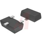
封装:
SOT-723-3
描述:
NPN 晶体管,ON Semiconductor### 标准带 S 或 NSV 前缀的制造商部件号具有汽车资格,符合 AEC-Q101 标准。### 数字晶体管,On Semiconductor配备电阻器的双极性晶体管也称为数字晶体管或偏流电阻器的晶体管,包含一个或两个集成电阻器。 单一系列输入电阻器,或两个电阻器的分压器能直接从数字源驱动这些设备。 提供单和双晶体管型号。
Pictures:
3D模型
符号图
焊盘图
引脚图
产品图
页面导航:
引脚图在P1Hot
封装尺寸在P7P8P9P10P11P12
焊盘布局在P7P8P9P10P11P12
型号编码规则在P1P2P12
标记信息在P1P2P12
封装信息在P2
技术参数、封装参数在P2
应用领域在P1
电气规格在P4
导航目录
DTC124EM3T5G数据手册
Page:
of 12 Go
若手册格式错乱,请下载阅览PDF原文件
© Semiconductor Components Industries, LLC, 2013
March, 2013 − Rev. 2
1 Publication Order Number:
DTC124E/D
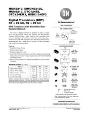
MUN2212, MMUN2212L,
MUN5212, DTC124EE,
DTC124EM3, NSBC124EF3
Digital Transistors (BRT)
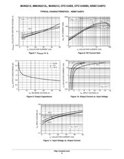
R1 = 22 kW, R2 = 22 kW
NPN Transistors with Monolithic Bias
Resistor Network
This series of digital transistors is designed to replace a single
device and its external resistor bias network. The Bias Resistor
Transistor (BRT) contains a single transistor with a monolithic bias
network consisting of two resistors; a series base resistor and a base−
emitter resistor. The BRT eliminates these individual components by
integrating them into a single device. The use of a BRT can reduce
both system cost and board space.
Features
• Simplifies Circuit Design
• Reduces Board Space
• Reduces Component Count
• S and NSV Prefix for Automotive and Other Applications Requiring
Unique Site and Control Change Requirements; AEC-Q101 Qualified
and PPAP Capable
• These Devices are Pb−Free, Halogen Free/BFR Free and are RoHS
Compliant
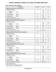
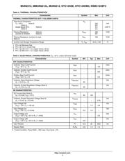
MAXIMUM RATINGS (T
A
= 25°C)
Rating
Symbol Max Unit
Collector−Base Voltage V
CBO
50 Vdc
Collector−Emitter Voltage V
CEO
50 Vdc
Collector Current − Continuous I
C
100 mAdc
Input Forward Voltage V
IN(fwd)
40 Vdc
Input Reverse Voltage V
IN(rev)
10 Vdc
Stresses exceeding Maximum Ratings may damage the device. Maximum
Ratings are stress ratings only. Functional operation above the Recommended
Operating Conditions is not implied. Extended exposure to stresses above the
Recommended Operating Conditions may affect device reliability.
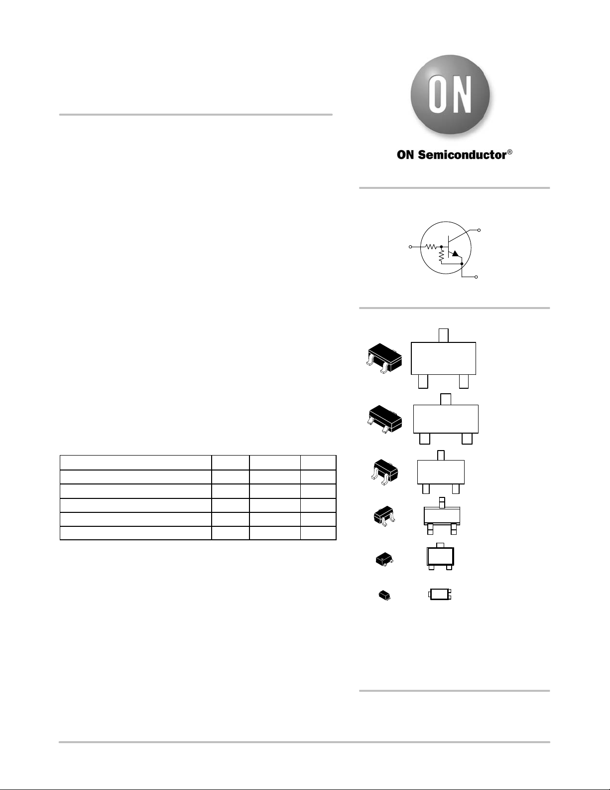
PIN 3
COLLECTOR
(OUTPUT)
PIN 2
EMITTER
(GROUND)
PIN 1
BASE
(INPUT)
R1
R2
See detailed ordering, marking, and shipping information in
the package dimensions section on page 2 of this data sheet.
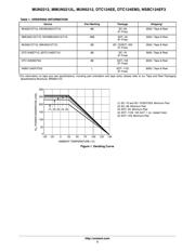
ORDERING INFORMATION
http://onsemi.com
SC−75
CASE 463
STYLE 1
MARKING DIAGRAMS
XXX = Specific Device Code
M = Date Code*
G =Pb−Free Package
(Note: Microdot may be in either location)
*Date Code orientation may vary depending
upon manufacturing location.
SC−59
CASE 318D
STYLE 1
SOT−23
CASE 318
STYLE 6
SC−70/SOT−323
CASE 419
STYLE 3
SOT−723
CASE 631AA
STYLE 1
SOT−1123
CASE 524AA
STYLE 1
XX MG
G
1
1
XXX MG
G
XX MG
G
1
XX M
1
X M
XX M
1
1
PIN CONNECTIONS
器件 Datasheet 文档搜索
AiEMA 数据库涵盖高达 72,405,303 个元件的数据手册,每天更新 5,000 多个 PDF 文件
