Datasheet 搜索 > FPGA芯片 > Altera(阿尔特拉) > EP1C12F324C7 数据手册 > EP1C12F324C7 数据手册 377/385 页

 器件3D模型
¥ 470.86
EP1C12F324C7 数据手册 - Altera(阿尔特拉)
制造商:
Altera(阿尔特拉)
分类:
FPGA芯片
封装:
FBGA-324
Pictures:
3D模型
符号图
焊盘图
引脚图
产品图
页面导航:
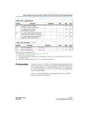
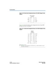
引脚图在P162P314P317P377Hot
典型应用电路图在P25P27P29P31P255P273
原理图在P22P141P341
封装尺寸在P12P117P377P383P384
型号编码规则在P11P117
功能描述在P21P148P149P150P152P336P338P340
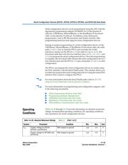
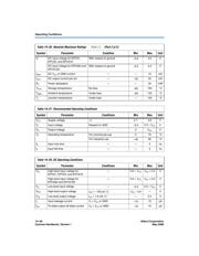
技术参数、封装参数在P85P86P87P88P89P90P94P113P114P142P224P225
应用领域在P102P203P228
电气规格在P225
导航目录
EP1C12F324C7数据手册
Page:
of 385 Go
若手册格式错乱,请下载阅览PDF原文件
Altera Corporation 14–43
May 2008 Cyclone Handbook, Volume 1
Serial Configuration Devices (EPCS1, EPCS4, EPCS16, EPCS64, and EPCS128) Data Sheet
Package
All serial configuration devices are available in 8-pin or 16-pin plastic
SOIC package.
f For more information on Altera device packaging including mechanical
drawing and specifications for this package, refer to the Altera Device
Package Information Data Sheet.
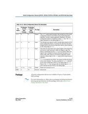
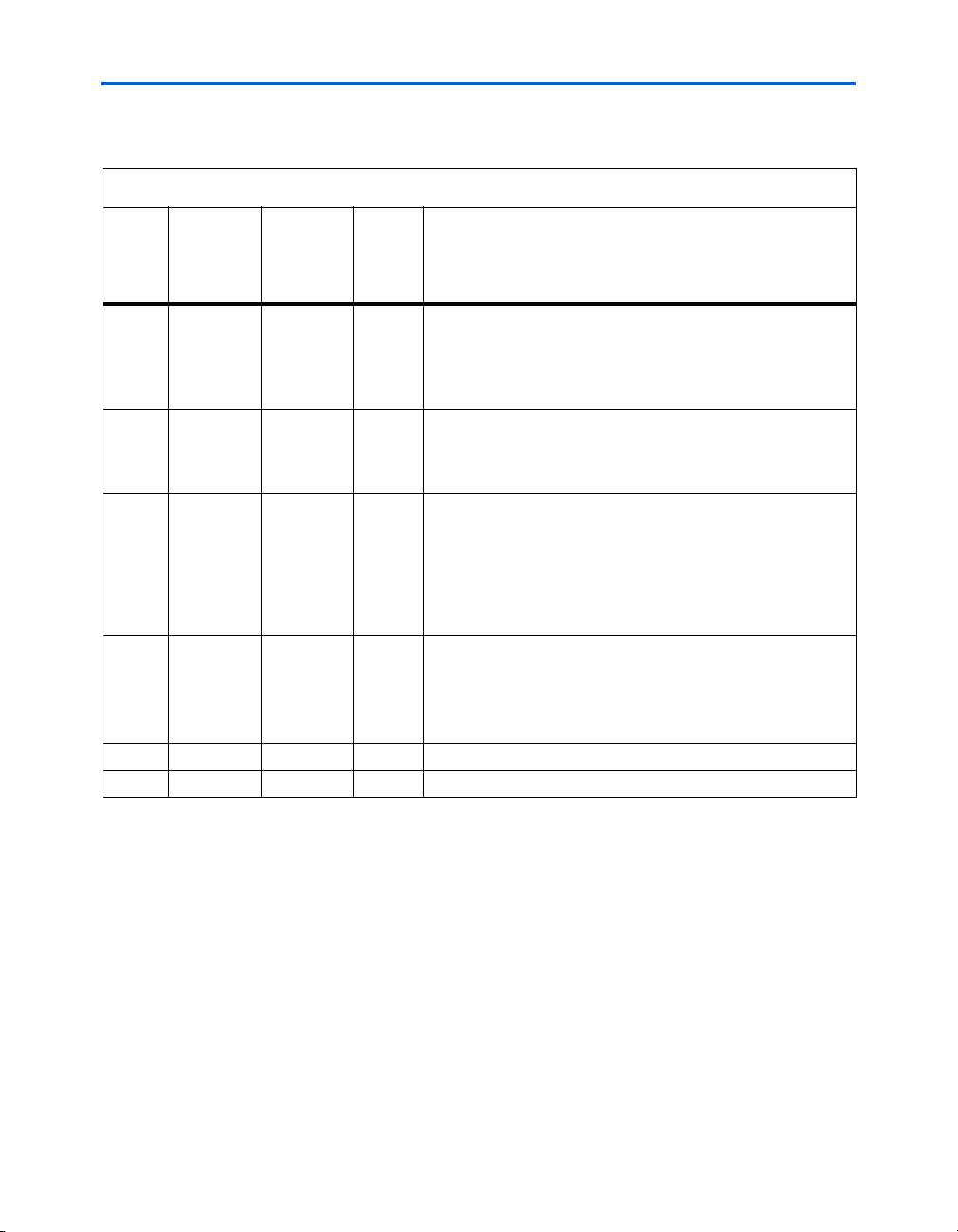
Table 14–31. Serial Configuration Device Pin Description
Pin
Name
Pin Number
in 8-Pin
SOIC
Package
Pin Number
in 16-Pin
SOIC
Package
Pin Type Description
DATA
2 8 Output
The
DATA output signal transfers data serially out of the serial
configuration device to the FPGA during read/configuration
operation. During a read/configuration operations, the serial
configuration device is enabled by pulling
nCS low. The DATA
signal transitions on the falling edge of
DCLK.
ASDI
5 15 Input The AS data input signal is used to transfer data serially into the
serial configuration device. It receives the data that should be
programmed into the serial configuration device. Data is latched
on the rising edge of
DCLK.
nCS
1 7 Input The active low chip select input signal toggles at the beginning
and end of a valid instruction. When this signal is high, the
device is deselected and the
DATA pin is tri-stated. When this
signal is low, it enables the device and puts the device in an
active mode. After power up, the serial configuration device
requires a falling edge on the
nCS signal before beginning any
operation.
DCLK
6 16 Input
DCLK is provided by the FPGA. This signal provides the timing
of the serial interface. The data presented on
ASDI is latched
to the serial configuration device on the falling edge of
DCLK.
Data on the
DATA pin changes after the falling edge of DCLK
and is latched into the FPGA on the falling edge.
V
CC
3, 7, 8 1, 2, 9 Power Power pins connect to 3.3 V.
GND 4 10 Ground Ground pin.
器件 Datasheet 文档搜索
AiEMA 数据库涵盖高达 72,405,303 个元件的数据手册,每天更新 5,000 多个 PDF 文件
