Datasheet 搜索 > FPGA芯片 > Altera(阿尔特拉) > EP1C4F400C8N 数据手册 > EP1C4F400C8N 数据手册 141/386 页
 器件3D模型
¥ 72.479
EP1C4F400C8N 数据手册 - Altera(阿尔特拉)
制造商:
Altera(阿尔特拉)
分类:
FPGA芯片
封装:
FBGA-400
描述:
可编程逻辑器件(CPLD/FPGA) EP1C4F400C8N FBGA-400
Pictures:
3D模型
符号图
焊盘图
引脚图
产品图
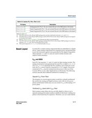
页面导航:
引脚图在P162P314P317P377Hot
典型应用电路图在P25P27P29P31P255P273
原理图在P22P141P341
封装尺寸在P12P117P377P383P384
型号编码规则在P11P117
功能描述在P21P148P149P150P152P336P338P340
技术参数、封装参数在P85P86P87P88P89P90P94P113P114P142P224P225
应用领域在P102P203P228
电气规格在P225
导航目录
EP1C4F400C8N数据手册
Page:
of 386 Go
若手册格式错乱,请下载阅览PDF原文件
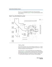
Altera Corporation 6–19
May 2008 Preliminary
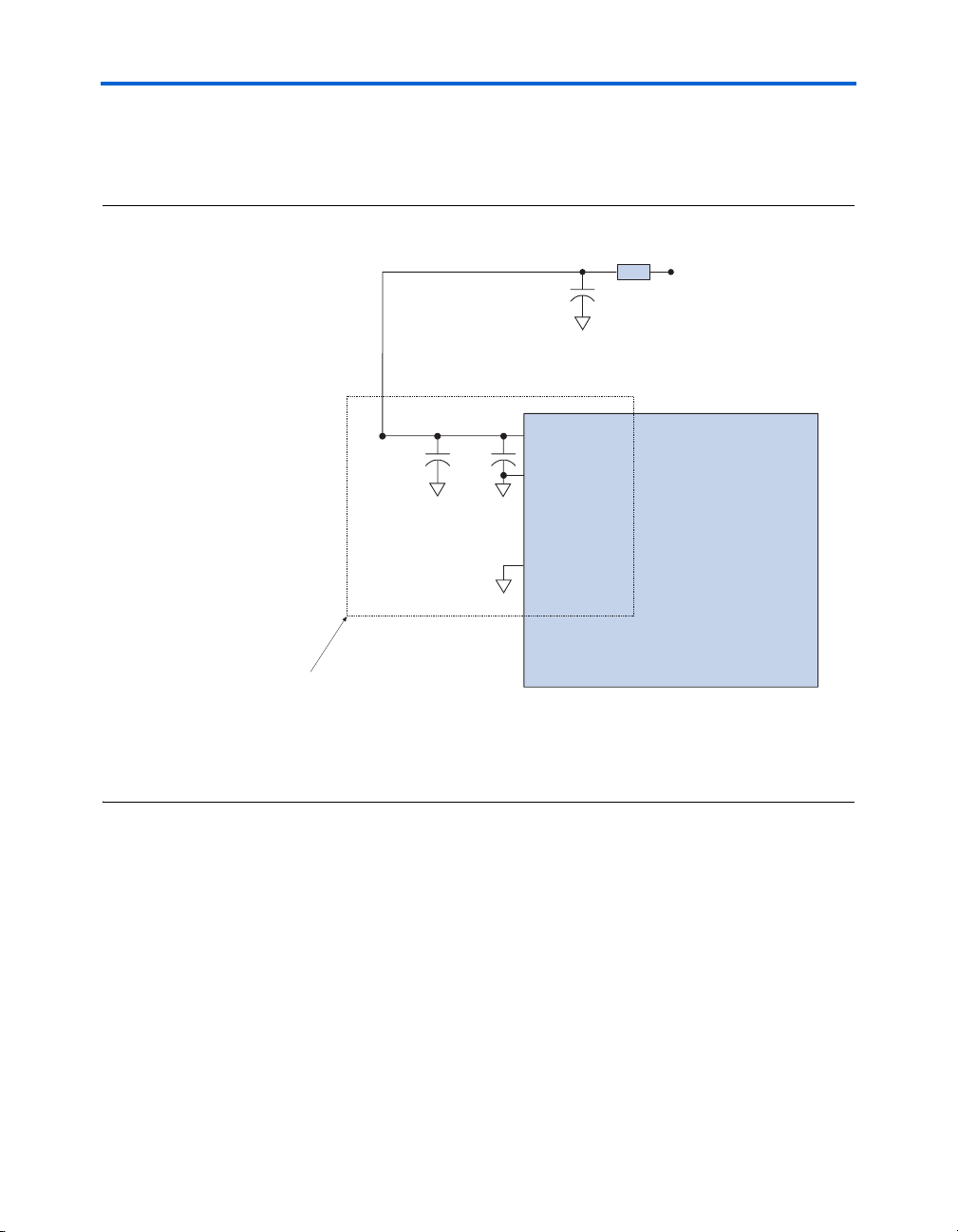
Board Layout
combination of ceramic capacitors located as close as possible to the
Cyclone FPGA. You can connect the GNDA pins directly to the same GND
plane as the digital GND of the device.
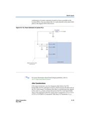
Figure 6–8. PLL Power Schematic for Cyclone PLLs
f For more information about board design guidelines, refer to
AN 75: High-Speed Board Designs.
Jitter Considerations
If the input clocks have any low-frequency jitter (below the PLL
bandwidth), the PLL attempts to track it, which increases the jitter seen at
the PLL clock output. To minimize this effect, avoid placing noisy signals
in the same V
CCIO
bank as those that power the PLL clock input buffer.
This is only important if the PLL input clock is assigned to 3.3-V or 2.5-V
LVTTL or LVCMOS I/O standards. With these I/O standards, V
CCIO
Cyclone Device
1.5-V Supply
Ferrite Bead
10 μF
GND
Repeat for each PLL power
and ground set
GND
GND
GND
PLL<#>_VCCA
PLL<#>_GNDA
PLL<#>_GNDG
-1 μF .001 μF
器件 Datasheet 文档搜索
AiEMA 数据库涵盖高达 72,405,303 个元件的数据手册,每天更新 5,000 多个 PDF 文件
