Datasheet 搜索 > FPGA芯片 > Altera(阿尔特拉) > EP1S25F672C8 数据手册 > EP1S25F672C8 数据手册 1/276 页
 器件3D模型
¥ 4616.39
EP1S25F672C8 数据手册 - Altera(阿尔特拉)
制造商:
Altera(阿尔特拉)
分类:
FPGA芯片
封装:
FBGA-672
Pictures:
3D模型
符号图
焊盘图
引脚图
产品图
页面导航:
引脚图在P91P92Hot
典型应用电路图在P20P22P24P26
原理图在P16P69P70
封装尺寸在P275
型号编码规则在P275P276
封装信息在P276
功能描述在P15P16
技术参数、封装参数在P3P171P173P174P176P177P178P179P180P181P182P183
应用领域在P190P191
电气规格在P168

导航目录
EP1S25F672C8数据手册
Page:
of 276 Go
若手册格式错乱,请下载阅览PDF原文件
Altera Corporation Section I–1
Section I. Stratix Device
Family Data Sheet
This section provides the data sheet specifications for Stratix
®
devices.
They contain feature definitions of the internal architecture,
configuration and JTAG boundary-scan testing information, DC
operating conditions, AC timing parameters, a reference to power
consumption, and ordering information for Stratix devices.
This section contains the following chapters:
■ Chapter 1, Introduction
■ Chapter 2, Stratix Architecture
■ Chapter 3, Configuration & Testing
■ Chapter 4, DC & Switching Characteristics
■ Chapter 5, Reference & Ordering Information
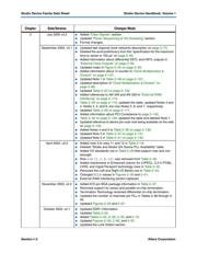
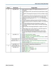
Revision History
The table below shows the revision history for Chapters 1 through 5.
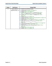
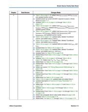
Chapter Date/Version Changes Made
1 July 2005, v3.2 ● Minor content changes.
September 2004, v3.1
● Updated Table 1–6 on page 1–5.
April 2004, v3.0
● Main section page numbers changed on first page.
● Changed PCI-X to PCI-X 1.0 in “Features” on page 1–2.
● Global change from SignalTap to SignalTap II.
● The DSP blocks in “Features” on page 1–2 provide dedicated
implementation of multipliers that are now “faster than 300 MHz.”
January 2004, v2.2
● Updated -5 speed grade device information in Table 1-6.
October 2003, v2.1
● Add -8 speed grade device information.
July 2003, v2.0
● Format changes throughout chapter.
器件 Datasheet 文档搜索
AiEMA 数据库涵盖高达 72,405,303 个元件的数据手册,每天更新 5,000 多个 PDF 文件
