Datasheet 搜索 > FPGA芯片 > Altera(阿尔特拉) > EP2C8T144I8N 数据手册 > EP2C8T144I8N 数据手册 86/168 页

 器件3D模型
¥ 99.451
EP2C8T144I8N 数据手册 - Altera(阿尔特拉)
制造商:
Altera(阿尔特拉)
分类:
FPGA芯片
封装:
TQFP-144
描述:
ALTERA EP2C8T144I8N 芯片, FPGA, CYCLONE II, 8K单元, TQFP144
Pictures:
3D模型
符号图
焊盘图
引脚图
产品图
页面导航:
典型应用电路图在P14P16P18
原理图在P14P86
型号编码规则在P167
功能描述在P13
技术参数、封装参数在P63P78P83P84P86P91P93P95P97P99P101P102
应用领域在P105P106P107P108P167

导航目录
EP2C8T144I8N数据手册
Page:
of 168 Go
若手册格式错乱,请下载阅览PDF原文件
4–4 Altera Corporation
Cyclone II Device Handbook, Volume 1 February 2007
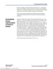
Hot-Socketing Feature Implementation in Cyclone II Devices
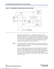
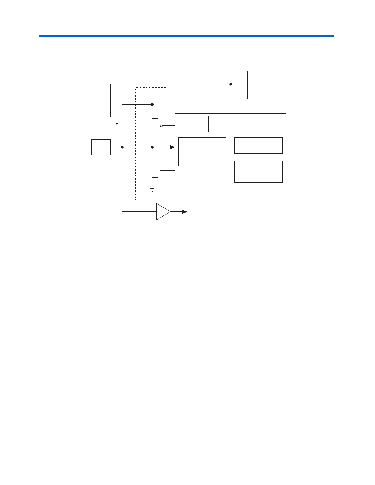
Figure 4–1. Hot-Socketing Circuit Block Diagram for Cyclone II Devices
The POR circuit monitors V
CCINT
voltage level and keeps I/O pins
tri-stated until the device is in user mode. The weak pull-up resistor (R)
from the I/O pin to V
CCIO
keeps the I/O pins from floating. The voltage
tolerance control circuit permits the I/O pins to be driven by 3.3 V before
V
CCIO
and/or V
CCINT
are powered, and it prevents the I/O pins from
driving out when the device is not in user mode.
f For more information, see the DC Characteristics & Timing Specifications
chapter in Volume 1 of the Cyclone II Device Handbook for the value of the
internal weak pull-up resistors.
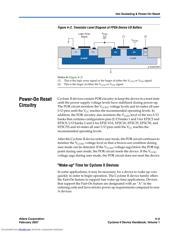
Figure 4–2 shows a transistor level cross section of the Cyclone II device
I/O buffers. This design ensures that the output buffers do not drive
when V
CCIO
is powered before V
CCINT
or if the I/O pad voltage is higher
than V
CCIO
. This also applies for sudden voltage spikes during hot
socketing. The V
PAD
leakage current charges the voltage tolerance control
circuit capacitance.
Output Enable
Output
Hot Socket
Output
Pre-Driver
Voltage
Tolerance
Control
Power-On
Reset
Monitor
Weak
Pull-Up
Resistor
PAD
Input Buffer
to Logic Array
R
Downloaded from Elcodis.com electronic components distributor
器件 Datasheet 文档搜索
AiEMA 数据库涵盖高达 72,405,303 个元件的数据手册,每天更新 5,000 多个 PDF 文件
