Datasheet 搜索 > Intel(英特尔) > EP3C5F256I7N 数据手册 > EP3C5F256I7N 数据手册 4/34 页

¥ 341.122
EP3C5F256I7N 数据手册 - Intel(英特尔)
制造商:
Intel(英特尔)
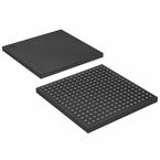
封装:
LBGA-256
Pictures:
3D模型
符号图
焊盘图
引脚图
产品图
页面导航:
技术参数、封装参数在P1P2P6P9P10P11P12P13P14P15P16P17
电气规格在P1P2P3P4P5P6P7P8P9P10P11P12
导航目录
EP3C5F256I7N数据手册
Page:
of 34 Go
若手册格式错乱,请下载阅览PDF原文件
1–4 Chapter 1: Cyclone III Device Datasheet
Electrical Characteristics
Cyclone III Device Handbook July 2012 Altera Corporation
Volume 2
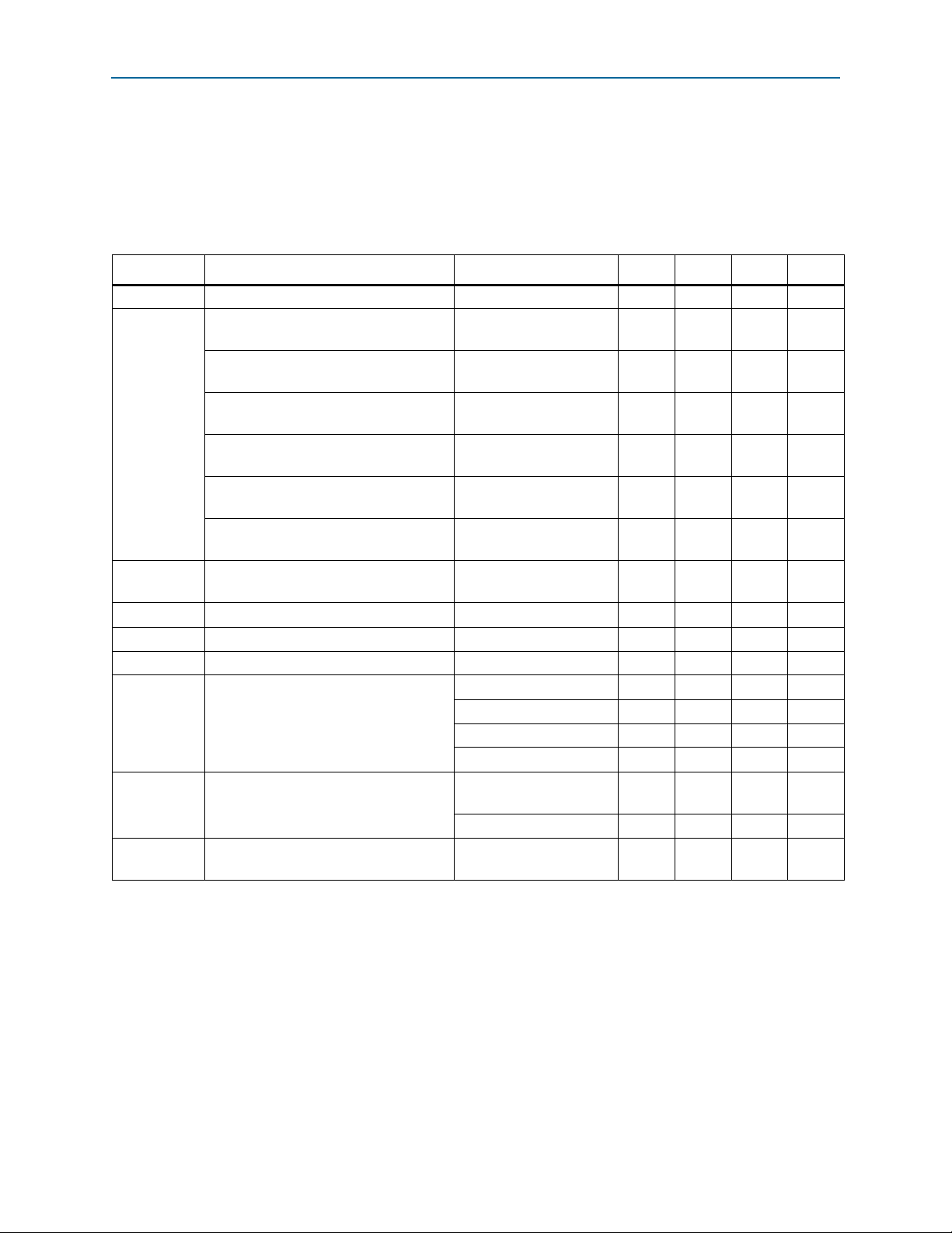
Recommended Operating Conditions
This section lists the functional operation limits for AC and DC parameters for
Cyclone III devices. The steady-state voltage and current values expected from
Cyclone III devices are provided in Table 1–3. All supplies must be strictly monotonic
without plateaus.
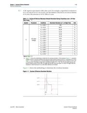
Table 1–3. Cyclone III Devices Recommended Operating Conditions
(1),
(2)
Symbol Parameter Conditions Min Typ Max Unit
V
CCINT
(3)
Supply voltage for internal logic — 1.15 1.2 1.25 V
V
CCIO
(3),
(4)
Supply voltage for output buffers, 3.3-V
operation
— 3.135 3.3 3.465 V
Supply voltage for output buffers, 3.0-V
operation
— 2.85 3 3.15 V
Supply voltage for output buffers, 2.5-V
operation
— 2.375 2.5 2.625 V
Supply voltage for output buffers, 1.8-V
operation
— 1.71 1.8 1.89 V
Supply voltage for output buffers, 1.5-V
operation
— 1.425 1.5 1.575 V
Supply voltage for output buffers, 1.2-V
operation
— 1.14 1.2 1.26 V
V
CCA
(3)
Supply (analog) voltage for PLL
regulator
— 2.375 2.5 2.625 V
V
CCD_PLL
(3)
Supply (digital) voltage for PLL — 1.15 1.2 1.25 V
V
I
Input voltage — –0.5 — 3.6 V
V
O
Output voltage — 0 — V
CCIO
V
T
J
Operating junction temperature
For commercial use 0 — 85 °C
For industrial use –40 — 100 °C
For extended temperature –40 — 125 °C
For automotive use –40 — 125 °C
t
RAMP
Power supply ramp time
Standard power-on reset
(POR)
(5)
50 µs — 50 ms —
Fast POR
(6)
50 µs — 3 ms —
I
Diode
Magnitude of DC current across
PCI-clamp diode when enabled
———10mA
Notes to Table 1–3:
(1) V
CCIO
for all I/O banks must be powered up during device operation. All V
CCA
pins must be powered to 2.5 V (even when PLLs are not used), and
must be powered up and powered down at the same time.
(2) V
CCD_PLL
must always be connected to V
CCINT
through a decoupling capacitor and ferrite bead.
(3) The V
CC
must rise monotonically.
(4) All input buffers are powered by the V
CCIO
supply.
(5) POR time for Standard POR ranges between 50–200 ms. Each individual power supply should reach the recommended operating range within
50 ms.
(6) POR time for Fast POR ranges between 3–9 ms. Each individual power supply should reach the recommended operating range within 3 ms.
器件 Datasheet 文档搜索
AiEMA 数据库涵盖高达 72,405,303 个元件的数据手册,每天更新 5,000 多个 PDF 文件
