Datasheet 搜索 > MOS管 > Fairchild(飞兆/仙童) > FCP7N60 数据手册 > FCP7N60 数据手册 1/11 页

¥ 12.904
FCP7N60 数据手册 - Fairchild(飞兆/仙童)
制造商:
Fairchild(飞兆/仙童)
分类:
MOS管
封装:
TO-220-3
描述:
SuperFET® 和 SuperFET® II N 通道 MOSFET,Fairchild SemiconductorFairchild 使用超级结技术增加了 SuperFET® II 高电压功率 MOSFET 系列。 它提供最佳坚固主体二极管性能,适用于要求高功率密度、系统效率和可靠性的交流-直流开关模式电源 (SMPS) 应用,如服务器、电信、计算、工业电源、UPS/ESS、太阳能逆变器和照明应用。 利用先进的电荷平衡技术,设计人员可实现更高效经济的高性能解决方案,可占用更少板空间并提高可靠性。### MOSFET 晶体管,Fairchild SemiconductorFairchild 提供大量 MOSFET 设备组合,包括高电压 (>250V) 低电压 (Fairchild MOSFET 通过降低电压峰值和过冲提供极佳的设计可靠性,以减少结电容和反向恢复电荷,无需额外外部元件即可保持系统启动和运行更长时间。
Pictures:
3D模型
符号图
焊盘图
引脚图
产品图
页面导航:
导航目录
FCP7N60数据手册
Page:
of 11 Go
若手册格式错乱,请下载阅览PDF原文件
November 2013
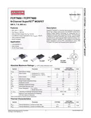
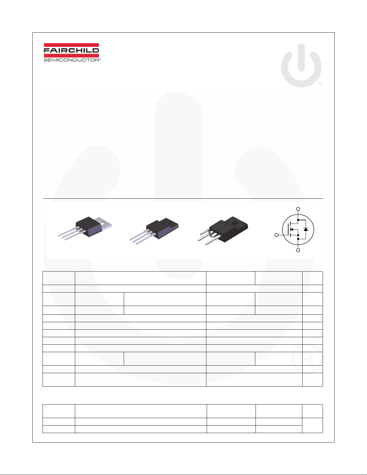
FCP7N60 / FCPF7N60 — N-Channel SuperFET
®
MOSFET
©2005 Fairchild Semiconductor Corporation
FCP7N60 / FCPF7N60 Rev. C1
www.fairchildsemi.com
1
TO-220
G
D
S
TO-220F
G
D
S
G
S
D
FCP7N60 / FCPF7N60
N-Channel SuperFET
®
MOSFET
600 V, 7 A, 600 mΩ
Features
•650 V @ T
J
= 150
o
C
•Typ. R
DS(on)
= 530 mΩ
• Ultra Low Gate Charge (Typ. Q
g
= 23 nC)
• Low Effective Output Capacitance (Typ. C
oss(eff.)
= 60 pF)
• 100% Avalanche Tested
•RoHS Compliant
Application
• LCD/LED/PDP TV
• Solar Inverter
• AC-DC Power Supply
Description
SuperFET
®
MOSFET is Fairchild Semiconductor’s first genera-
tion of high voltage super-junction (SJ) MOSFET family that is
utilizing charge balance technology for outstanding low on-
resistance and lower gate charge performance. This technology
is tailored to minimize conduction loss, provide superior switch-
ing performance, dv/dt rate and higher avalanche energy. Con-
sequently, SuperFET MOSFET is very suitable for the switching
power applications such as PFC, server/telecom power, FPD
TV power, ATX power and industrial power applications.
Absolute Maximum Ratings T
C
= 25
o
C unless otherwise noted.
Thermal Characteristics
Symbol Parameter FCP7N60
FCPF7N60 /
FCPF7N60YDTU
Unit
V
DSS
Drain-Source Voltage 600 V
I
D
Drain Current - Continuous (T
C
= 25°C)
- Continuous (T
C
= 100°C)
7
4.4
7*
4.4*
A
A
I
DM
Drain Current - Pulsed
(Note 1)
21 21*
A
V
GSS
Gate-Source voltage ± 30 V
E
AS
Single Pulsed Avalanche Energy
(Note 2)
230 mJ
I
AR
Avalanche Current
(Note 1)
7A
E
AR
Repetitive Avalanche Energy
(Note 1)
8.3 mJ
dv/dt Peak Diode Recovery dv/dt
(Note 3)
4.5 V/ns
P
D
Power Dissipation (T
C
= 25°C)
- Derate Above 25°C
83
0.67
31
0.25
W
W/°C
T
J,
T
STG
Operating and Storage Temperature Range -55 to +150 °C
T
L
Maximum Lead Temperature for Soldering,
1/8” from Case for 5 Seconds
300 °C
Symbol Parameter FCP7N60
FCPF7N60 /
FCPF7N60YDTU
Unit
R
θJC
Thermal Resistance, Junction-to-Case, Max. 1.5 4.0
°C/W
R
θJA
Thermal Resistance, Junction-to-Ambient, Max. 62.5 62.5
*Drain current limited by maximum junction temperature.
G
S
D
TO-220F
Y-formed
器件 Datasheet 文档搜索
AiEMA 数据库涵盖高达 72,405,303 个元件的数据手册,每天更新 5,000 多个 PDF 文件
