Datasheet 搜索 > TI(德州仪器) > FDC1004DSCR 数据手册 > FDC1004DSCR 数据手册 10/33 页

¥ 52.103
FDC1004DSCR 数据手册 - TI(德州仪器)
制造商:
TI(德州仪器)
封装:
WFDFN-10
描述:
具有源屏蔽驱动器的 4 通道、16 位、电感数字转换器 10-WSON -40 to 125
Pictures:
3D模型
符号图
焊盘图
引脚图
产品图
页面导航:
引脚图在P4Hot
典型应用电路图在P1P21P22
原理图在P10
封装尺寸在P25P27P28P30
焊盘布局在P31
标记信息在P25
封装信息在P24P25P26P27P28
技术参数、封装参数在P5P6P16
应用领域在P1P10P20P24P33
电气规格在P6P16
导航目录
FDC1004DSCR数据手册
Page:
of 33 Go
若手册格式错乱,请下载阅览PDF原文件
CAPACITANCE
TO DIGITAL
CONVERTER
I
2
C
FDC1004
SDA
SCL
VDD
GND
OFFSET
&
GAIN
CALIBRATION
CONFIGURATION REGISTERS
&
DATA REGISTERS
CAPDAC
M
U
X
EXCITATION
M
U
X
CIN1
CIN2
CIN3
CIN4
SHLD2
SHLD1
CHA
CHB
FDC1004
SNOSCY5B –AUGUST 2014–REVISED APRIL 2015
www.ti.com
8 Detailed Description
8.1 Overview
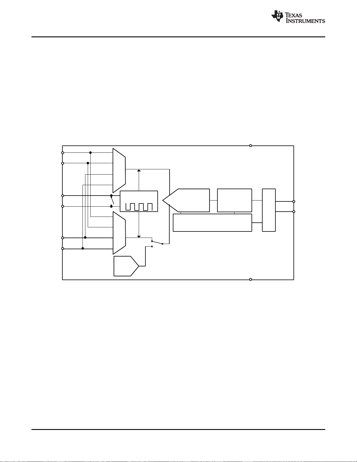
The FDC1004 is a high-resolution, 4-channel capacitance-to-digital converter for implementing capacitive
sensing solutions. Each channel has a full scale range of ±15 pF and can handle a sensor offset capacitance of
up to 100 pF, which can be either programmed internally or can be an external capacitor for tracking
environmental changes over time and temperature. The large offset capacitance capability allows for the use of
remote sensors. The FDC1004 also includes shield drivers for sensor shields, which can reduce EMI interference
and help focus the sensing direction of a capacitive sensor. The small footprint of the FDC1004 allows for use in
space-constrained applications. For more information on the basics of capacitive sensing and applications, refer
to FDC1004: Basics of Capacitive Sensing and Applications application note (SNOA927).
8.2 Functional Block Diagram
8.3 Feature Description
8.3.1 The Shield
The FDC1004 measures capacitance between CINn and ground. That means any capacitance to ground on
signal path between the FDC1004 CINn pins and sensor is included in the FDC1004 conversion result.
In some applications, the parasitic capacitance of the sensor connections can be larger than the capacitance of
the sensor. If that parasitic capacitance is stable, it can be treated as a constant capacitive offset. However, the
parasitic capacitance of the sensor connections can have significant variation due to environmental changes
(such as mechanical movement, temperature shifts, humidity changes). These changes are seen as drift in the
conversion result and may significantly compromise the system accuracy.
To eliminate the CINn parasitic capacitance to ground, the FDC1004 SHLDx signals can be used for shielding
the connection between the sensor and CINn. The SHLDx output is the same signal waveform as the excitation
of the CINn pin; the SHLDx is driven to the same voltage potential as the CINn pin. Therefore, there is no current
between CINn and SHLDx pins, and any capacitance between these pins does not affect the CINn charge
transfer. Ideally, the CINn to SHLD capacitance does not have any contribution to the FDC1004 result.
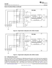
In differential measurements, SHLD1 is assigned to CHn and SHLD2 is assigned to CHm, where n < m. For
instance in the measurement CIN1 – CIN2, where CHA = CIN1 and CHB = CIN2 (see Table 4), SHDL1 is
assigned to CIN1 and SHDL2 is assigned to CIN2.
10 Submit Documentation Feedback Copyright © 2014–2015, Texas Instruments Incorporated
Product Folder Links: FDC1004
器件 Datasheet 文档搜索
AiEMA 数据库涵盖高达 72,405,303 个元件的数据手册,每天更新 5,000 多个 PDF 文件
