Datasheet 搜索 > MOS管 > Fairchild(飞兆/仙童) > FDMS8090 数据手册 > FDMS8090 数据手册 1/7 页


¥ 9.96
FDMS8090 数据手册 - Fairchild(飞兆/仙童)
制造商:
Fairchild(飞兆/仙童)
分类:
MOS管
封装:
Power-56-8
描述:
PowerTrench® 双 N 通道 MOSFET,Fairchild SemiconductorPowerTrench® MOSFET 是优化的电源开关,可提供高系统效率和功率密度。 它们组合了小栅极电荷 (Qg)、小反向恢复电荷 (Qrr) 和软性反向恢复主体二极管,有助于快速切换交流/直流电源中的同步整流。 最新的 PowerTrench® MOSFET 采用屏蔽栅极结构,可提供电荷平衡。 利用这一先进技术,这些设备的 FOM(品质因素)显著低于前一代的 FOM。 PowerTrench® MOSFET 的软性主体二极管性能可无需缓冲电路或替换更高额定电压的 MOSFET。### MOSFET 晶体管,Fairchild SemiconductorFairchild 提供大量 MOSFET 设备组合,包括高电压 (>250V) 低电压 (Fairchild MOSFET 通过降低电压峰值和过冲提供极佳的设计可靠性,以减少结电容和反向恢复电荷,无需额外外部元件即可保持系统启动和运行更长时间。
Pictures:
3D模型
符号图
焊盘图
引脚图
产品图
页面导航:

导航目录
FDMS8090数据手册
Page:
of 7 Go
若手册格式错乱,请下载阅览PDF原文件
April 2013
FDMS8090 PowerTrench
®
Symmetrical Dual
©2012 Fairchild Semiconductor Corporation 1 www.fairchildsemi.com
FDMS8090 Rev.C1
Bottom
Top
G1
S1
S1
S1
D1
D2
G2
S2
S2
S2
G2
S2
S2
S2
G1
S1 S1
S1
Pin 1
Pin 1
1
2
3
4
8
7
6
5
Contact to D1
(backside)
Q1 Q2
Contact to D2
(backside)
Power 56
FDMS8090
PowerTrench
®
Symmetrical Dual
100 V N-Channel MOSFET
Features
Max r
DS(on)
= 13 mΩ at V
GS
= 10 V, I
D
= 10 A
Max r
DS(on)
= 20 mΩ at V
GS
= 6 V, I
D
= 8 A
Low inductance packaging shortens rise/fall times, resulting in
lower switching losses
MOSFET integration enables optimum layout for lower circuit
inductance and reduced switch node ringing
100% UIL tested
RoHS Compliant
General Description
This device includes two fast switching (Qgd minimized) 100V
N-Channel MOSFETs in a dual Power 56 (5 mm X 6 mm MLP)
package. The package is enhanced for exceptional thermal
performance.
Applications
Bridge Topologies
Synchronous Rectifier Pair
Motor Drives
MOSFET Maximum Ratings T
A
= 25 °C unless otherwise noted
Thermal Characteristics
Package Marking and Ordering Information
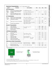
Symbol Parameter Ratings Units
V
DS
Drain to Source Voltage 100 V
V
GS
Gate to Source Voltage ±20 V
I
D
Drain Current -Continuous T
C
= 25 °C 40
A -Continuous T
A
= 25 °C (Note 1a) 10
-Pulsed (Note 4) 120
E
AS
Single Pulse Avalanche Energy (Note 3) 253 mJ
P
D
Power Dissipation T
C
= 25 °C 59
W
Power Dissipation T
A
= 25 °C (Note 1a) 2.2
T
J
, T
STG
Operating and Storage Junction Temperature Range -55 to +150 °C
R
θJC
Thermal Resistance, Junction to Case 2.1
°C/W
R
θJA
Thermal Resistance, Junction to Ambient (Note 1a) 55
Device Marking Device Package Reel Size Tape Width Quantity
FDMS8090 FDMS8090 Power 56 13 ’’ 12
mm 3000 units
器件 Datasheet 文档搜索
AiEMA 数据库涵盖高达 72,405,303 个元件的数据手册,每天更新 5,000 多个 PDF 文件
