Datasheet 搜索 > MOS管 > Fairchild(飞兆/仙童) > FDS4685 数据手册 > FDS4685 数据手册 2/6 页

 器件3D模型
¥ 3.25
FDS4685 数据手册 - Fairchild(飞兆/仙童)
制造商:
Fairchild(飞兆/仙童)
分类:
MOS管
封装:
SOIC-8
描述:
FAIRCHILD SEMICONDUCTOR FDS4685. 晶体管, P沟道
Pictures:
3D模型
符号图
焊盘图
引脚图
产品图
页面导航:


导航目录
FDS4685数据手册
Page:
of 6 Go
若手册格式错乱,请下载阅览PDF原文件
©2005 Fairchild Semiconductor Corporation
1
www.fairchildsemi.com
June 2005
FDS4685 Rev. C(W)
FDS4685 40V P-Channel PowerTrench
®
MOSFET
FDS4685
40V P-Channel PowerTrench
®
MOSFET
Features
■
–8.2 A, –40 V R
DS(ON)
= 0.027
Ω
@ V
GS
= –10 V
R
DS(ON)
= 0.035
Ω
@ V
GS
= –4.5 V
■
Fast switching speed
■
High performance trench technology for extremely low
R
DS(ON)
■
High power and current handling capability
Applications
■
Power management
■
Load switch
■
Battery protection
General Description
This P-Channel MOSFET is a rugged gate version of Fairchild
Semiconductor’s advanced PowerTrench process. It has been
optimized for power management applications requiring a wide
range of gate drive voltage ratings (4.5V – 20V).
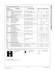
Absolute Maximum Ratings
T
A
= 25°C unless otherwise noted
Package Marking and Ordering Information
Symbol Parameter Ratings Units
V
DSS
Drain-Source Voltage –40 V
V
GSS
Gate-Source Voltage
±
20 V
I
D
Drain Current - Continuous (Note 1a) –8.2 A
- Pulsed –50
P
D
Power Dissipation for Single Operation (Note 1a) 2.5 W
(Note 1b) 1.4
(Note 1c) 1.2
T
J
, T
STG
Operating and Storage Junction Temperature Range –55 to +150
°
C
Thermal Characteristics
R
θ
JA
Thermal Resistance, Junction-to-Ambient (Note 1a) 50
°
C/W
R
θ
JA
Thermal Resistance, Junction-to-Ambient (Note 1c) 125
R
θ
JC
Thermal Resistance, Junction-to-Case (Note 1) 25
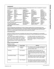
Device Marking Device Reel Size Tape width Quantity
FDS4685 FDS4685 13” 12mm 2500 units
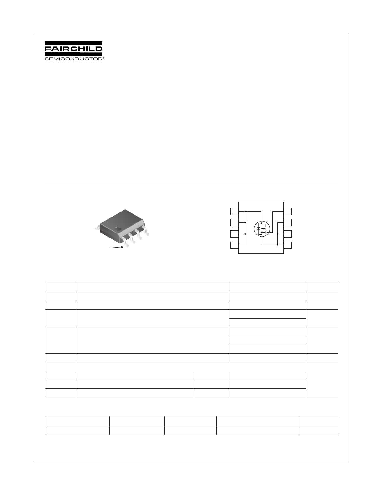
S
Pin 1
D
S
S
SO-8
D
D
D
G
5
6
7
8
4
3
2
1
器件 Datasheet 文档搜索
AiEMA 数据库涵盖高达 72,405,303 个元件的数据手册,每天更新 5,000 多个 PDF 文件
