Datasheet 搜索 > MOS管 > Fairchild(飞兆/仙童) > FDS6681Z 数据手册 > FDS6681Z 数据手册 2/8 页

 器件3D模型
¥ 9.182
FDS6681Z 数据手册 - Fairchild(飞兆/仙童)
制造商:
Fairchild(飞兆/仙童)
分类:
MOS管
封装:
SOIC-8
描述:
FAIRCHILD SEMICONDUCTOR FDS6681Z 晶体管, MOSFET, P沟道, 20 A, -30 V, 0.0038 ohm, -10 V, 1.8 V
Pictures:
3D模型
符号图
焊盘图
引脚图
产品图
页面导航:
导航目录
FDS6681Z数据手册
Page:
of 8 Go
若手册格式错乱,请下载阅览PDF原文件
IRF9310PbF
2 www.irf.com
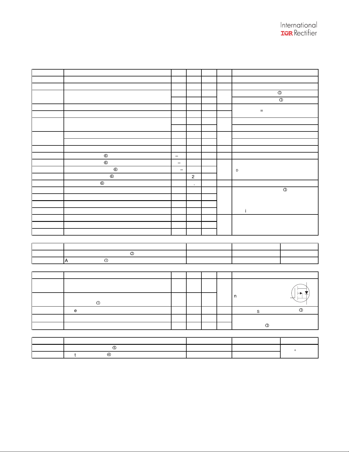
S
D
G
Notes:
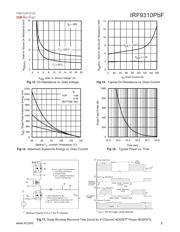
Repetitive rating; pulse width limited by max. junction temperature.
Starting T
J
= 25°C, L = 4.9mH, R
G
= 25Ω, I
AS
= -16A.
Pulse width ≤ 400µs; duty cycle ≤ 2%.
When mounted on 1 inch square copper board.
R
θ
is measured at T
J
of approximately 90°C.
For DESIGN AID ONLY, not subject to production testing.
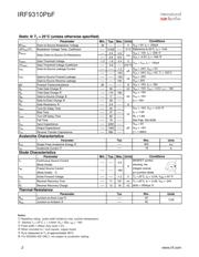
Static @ T
J
= 25°C (unless otherwise specified)
Parameter Min. Typ. Max. Units
BV
DSS
Drain-to-Source Breakdown Voltage -30 ––– ––– V
∆Β
V
DSS
/
∆
T
J
Breakdown Voltage Temp. Coefficient ––– 0.020 ––– V/°C
R
DS(on)
––– 3.9 4.6
––– 5.8 6.8
V
GS(th)
Gate Threshold Voltage -1.3 -1.8 -2.4 V
∆
V
GS(th)
Gate Threshold Voltage Coefficient ––– -5.8 ––– mV/°C
I
DSS
Drain-to-Source Leakage Current ––– ––– -1.0
––– ––– -150
I
GSS
Gate-to-Source Forward Leakage ––– ––– -100
Gate-to-Source Reverse Leakage ––– ––– 100
gfs Forward Transconductance 39 ––– ––– S
Q
g
Total Gate Charge
h
––– 58 ––– nC
V
DS
= -15V, V
GS
= -4.5V, I
D
= - 16A
Q
g
Total Gate Charge
h
––– 110 165
Q
gs
Gate-to-Source Charge
h
––– 17 –––
Q
gd
Gate-to-Drain Charge
h
––– 28 –––
R
G
Gate Resistance
h
––– 2.8 –––
Ω
t
d(on)
Turn-On Delay Time ––– 25 –––
t
r
Rise Time ––– 47 –––
t
d(off)
Turn-Off Delay Time ––– 65 –––
t
f
Fall Time ––– 70 –––
C
iss
Input Capacitance ––– 5250 –––
C
oss
Output Capacitance ––– 1300 –––
C
rss
Reverse Transfer Capacitance ––– 880 –––
Avalanche Characteristics
Parameter Units
E
AS
Single Pulse Avalanche Energy
d
mJ
I
AR
Avalanche Current
c
A
Diode Characteristics
Parameter Min. Typ. Max. Units
I
S
Continuous Source Current
(Body Diode)
I
SM
Pulsed Source Current
(Body Diode)
c
V
SD
Diode Forward Voltage ––– ––– -1.2 V
t
rr
Reverse Recovery Time ––– 71 107 ns
Q
rr
Reverse Recovery Charge ––– 12 18 nC
Thermal Resistance
Parameter Units
R
θJL
Junction-to-Drain Lead
g
R
θJA
Junction-to-Ambient
f
Typ.
–––
–––
°C/W
Max.
20
50
Static Drain-to-Source On-Resistance
A
––– –––
––– –––
-2.5
-160
nA
nC
ns
pF
–––
Typ.
–––
R
G
= 1.8Ω
V
DS
= -10V, I
D
= -16A
V
DS
= -24V, V
GS
= 0V, T
J
= 125°C
V
DD
= -15V, V
GS
= -4.5V
e
I
D
= -1.0A
V
DS
= -15V
V
GS
= -20V
V
GS
= 20V
V
GS
= -10V
m
Ω
µA
T
J
= 25°C, I
F
= -2.5A, V
DD
= -24V
di/dt = 100A/µs
e
T
J
= 25°C, I
S
= -2.5A, V
GS
= 0V
e
showing the
integral reverse
p-n junction diode.
MOSFET symbol
I
D
= -16A
V
DS
= -24V, V
GS
= 0V
Conditions
V
GS
= 0V, I
D
= -250µA
Reference to 25°C, I
D
= -1mA
V
GS
= -10V, I
D
= -20A
e
V
DS
= V
GS
, I
D
= -100µA
V
GS
= -4.5V, I
D
= -16A
e
Conditions
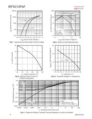
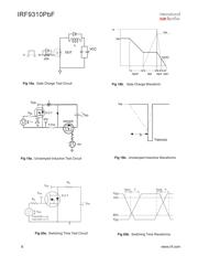
See Figs. 20a &20b
Max.
630
-16
ƒ = 1.0MHz
V
GS
= 0V
V
DS
= -15V
器件 Datasheet 文档搜索
AiEMA 数据库涵盖高达 72,405,303 个元件的数据手册,每天更新 5,000 多个 PDF 文件
