Datasheet 搜索 > 存储芯片 > Cypress Semiconductor(赛普拉斯) > FM25W256-GTR 数据手册 > FM25W256-GTR 数据手册 1/20 页
 器件3D模型
¥ 8.223
FM25W256-GTR 数据手册 - Cypress Semiconductor(赛普拉斯)
制造商:
Cypress Semiconductor(赛普拉斯)
分类:
存储芯片
封装:
SOIC-8
描述:
FM25W256 系列 256 Kb (32K x 8) 3.3V 表面贴装 SPI F-RAM 存储器 - SOIC-8
Pictures:
3D模型
符号图
焊盘图
引脚图
产品图
页面导航:
导航目录
FM25W256-GTR数据手册
Page:
of 20 Go
若手册格式错乱,请下载阅览PDF原文件
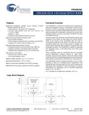
FM25W256
256-Kbit (32 K × 8) Serial (SPI) F-RAM
Cypress Semiconductor Corporation • 198 Champion Court • San Jose, CA 95134-1709 • 408-943-2600
Document Number: 001-84506 Rev. *E Revised August 11, 2015
64-Kbit (8 K × 8) Serial (SPI) F-RAM
Features
■ 256-Kbit ferroelectric random access memory (F-RAM)
logically organized as 32K × 8
❐ High-endurance 100 trillion (10
14
) read/writes
❐ 151-year data retention (See the Data Retention and
Endurance table)
❐ NoDelay™ writes
❐ Advanced high-reliability ferroelectric process
■ Very fast serial peripheral interface (SPI)
❐ Up to 20 MHz frequency
❐ Direct hardware replacement for serial flash and EEPROM
❐ Supports SPI mode 0 (0,0) and mode 3 (1,1)
■ Sophisticated write protection scheme
❐ Hardware protection using the Write Protect (WP) pin
❐ Software protection using Write Disable instruction
❐ Software block protection for 1/4, 1/2, or entire array
■ Low power consumption
❐ 250 μA active current at 1 MHz
❐ 15 μA (typ) standby current
■ Wide voltage operation: V
DD
= 2.7 V to 5.5 V
■ Industrial temperature: –40 °C to +85 °C
■ 8-pin small outline integrated circuit (SOIC) package
■ Restriction of hazardous substances (RoHS) compliant
Functional Overview
The FM25W256 is a 256-Kbit nonvolatile memory employing an
advanced ferroelectric process. A ferroelectric random access
memory or F-RAM is nonvolatile and performs reads and writes
similar to a RAM. It provides reliable data retention for 151 years
while eliminating the complexities, overhead, and system level
reliability problems caused by serial flash, EEPROM, and other
nonvolatile memories.
Unlike serial flash and EEPROM, the FM25W256 performs write
operations at bus speed. No write delays are incurred. Data is
written to the memory array immediately after each byte is
successfully transferred to the device. The next bus cycle can
commence without the need for data polling. In addition, the
product offers substantial write endurance compared with other
nonvolatile memories. The FM25W256 is capable of supporting
10
14
read/write cycles, or 100 million times more write cycles
than EEPROM.
These capabilities make the FM25W256 ideal for nonvolatile
memory applications requiring frequent or rapid writes.
Examples range from data collection, where the number of write
cycles may be critical, to demanding industrial controls where the
long write time of serial flash or EEPROM can cause data loss.
The FM25W256 provides substantial benefits to users of serial
EEPROM or flash as a hardware drop-in replacement. The
FM25W256 uses the high-speed SPI bus, which enhances the
high-speed write capability of F-RAM technology. The device
specifications are guaranteed over an industrial temperature
range of –40 °C to +85 °C.
For a complete list of related documentation, click here.
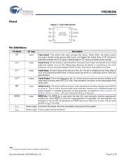
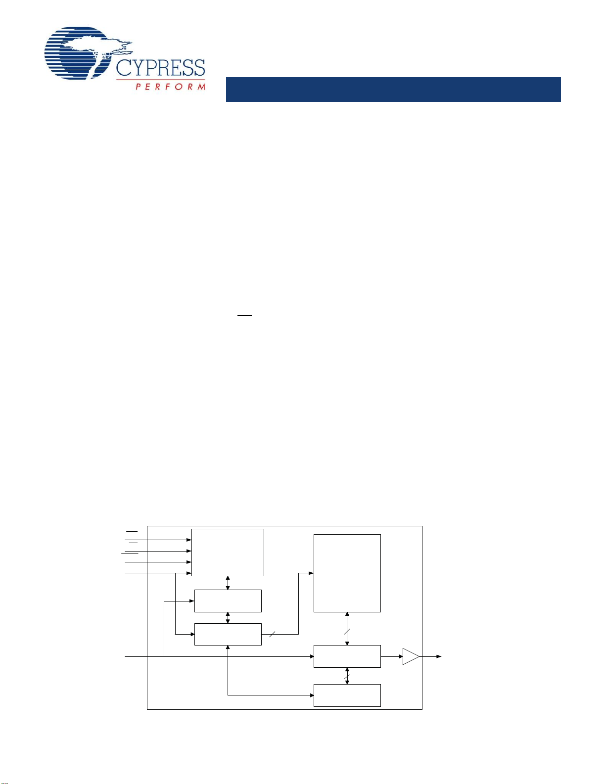
Instruction Decoder
Clock Generator
Control Logic
Write Protect
Instruction Register
Address Register
Counter
32 K x 8
F-RAM Array
15
Data I/ O Register
8
Nonvolatile Status
Register
3
WP
CS
HOLD
SCK
SOSI
Logic Block Diagram
器件 Datasheet 文档搜索
AiEMA 数据库涵盖高达 72,405,303 个元件的数据手册,每天更新 5,000 多个 PDF 文件
