Datasheet 搜索 > ON Semiconductor(安森美) > FSUSB30MUX 数据手册 > FSUSB30MUX 数据手册 4/17 页
 器件3D模型
¥ 1.097
FSUSB30MUX 数据手册 - ON Semiconductor(安森美)
制造商:
ON Semiconductor(安森美)
封装:
MSOP-10
描述:
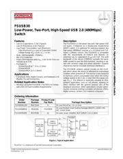
FSUSB30 系列 双刀双掷 4.3 V 480 Mbps 表面贴装 高速 USB 2.0 开关 - MSOP-10
Pictures:
3D模型
符号图
焊盘图
引脚图
产品图
页面导航:
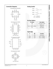
引脚图在P2Hot
典型应用电路图在P1
封装尺寸在P14P15P16
焊盘布局在P16
型号编码规则在P1
封装信息在P11P12P13
技术参数、封装参数在P3P11
应用领域在P1P10
电气规格在P4P5
导航目录
FSUSB30MUX数据手册
Page:
of 17 Go
若手册格式错乱,请下载阅览PDF原文件
© 2006 Fairchild Semiconductor Corporation www.fairchildsemi.com
FSUSB30 — Low-Power, Two-Port, High-Speed USB 2.0 (480Mbps) Switch
FSUSB30 Rev. 1.1.8 4
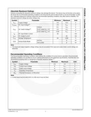
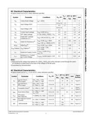
DC Electrical Characteristics
All typical values are at 25°C unless otherwise specified.
Notes:
3. Measured by the voltage drop between Dn, HSD1
n
, HSD2
n
pins at the indicated current through the switch.
On resistance is determined by the lower of the voltage on the two ports.
4.Guaranteed by characterization.
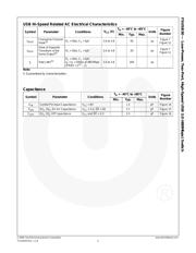
AC Electrical Characteristics
All typical values are for V
CC
= 3.3V at 25°C unless otherwise specified.
Symbol Parameter Conditions
V
CC
(V)
T
A
= 40°C to +85°C
Unit
Min. Typ. Max.
V
IK
Clamp Diode Voltage I
IN
= -18mA 3.0 -1.2 V
V
IH
Input Voltage HIGH
3.0 to 3.6 1.3 V
4.3 1.7 V
V
IL
Input Voltage LOW
3.0 to 3.6 0.5 V
4.3 0.7 V
I
IN
Control Input Leakage V
SW
= 0.0V to V
CC
4.3 -1.0 1.0 µA
I
OZ
OFF State Leakage 0 Dn, HSD1
n
, HSD2
n
V
CC
4.3 -2.0 2.0 µA
I
OFF
Power OFF Leakage
Current (D+, D–)
V
SW
= 0V to 4.3V, V
CC
= 0V 0 -2.0 2.0 µA
R
ON
Switch On Resistance
(3)
V
SW
= 0.4V, I
ON
= -8mA 3.0 6.5 10.0
V
SW
= 0V, I
O
= 30mA at 25°C 3.6 7.0
R
ON
Delta R
ON
(4)
V
SW
= 0.4V, I
ON
= -8mA 3.0 0.35
R
ON
Flatness R
ON
Flatness
(3)
V
SW
= 0.0V - 1.0V,
I
ON
= -8mA
3.0 2.0
I
CC
Quiescent Supply Current
V
CNTRL
= 0.0V or V
CC
,
I
OUT
= 0
4.3 1.0 µA
I
CCT
Increase in I
CC
Current
per Control Voltage
V
CNTRL
(control input) = 2.6V 4.3 10.0 µA
Symbol Parameter Conditions
V
CC
(V)
T
A
= 40°C to +85°C
Unit
Figure
Number
Min. Typ. Max.
t
ON
Turn-On Time S,
OE
to Output
HD1
n
, HD2
n
= 0.8V,
R
L
= 50, C
L
= 5pF
3.0 to 3.6 13 30 ns Figure 9
t
OFF
Turn-Off Time S,
OE
to Output
HD1
n
, HD2
n
= 0.8V,
R
L
= 50, C
L
= 5pF
3.0 to 3.6 12 25 ns Figure 9
t
PD
Propagation Delay
(4)
R
L
= 50, C
L
= 5pF 3.3 0.25 ns
Figure 7
Figure 8
t
BBM
Break-Before-Make
R
L
= 50, C
L
= 5pF,
V
IN
= 0.8V
3.0 to 3.6 2.0 6.5 ns Figure 10
O
IRR
Off Isolation
(Non-Adjacent)
f = 240MHz, R
T
= 50 3.0 to 3.6 -30 dB Figure 13
Xtalk
Non-Adjacent Channel
Crosstalk
R
T
= 50, f = 240MHz 3.0 to 3.6 -45 dB Figure 14
BW 3dB Bandwidth
R
T
= 50, C
L
= 0pF
3.0 to 3.6
720
MHz Figure 12
R
T
= 50, C
L
= 5pF 550
器件 Datasheet 文档搜索
AiEMA 数据库涵盖高达 72,405,303 个元件的数据手册,每天更新 5,000 多个 PDF 文件
