Datasheet 搜索 > 接口芯片 > FTDI Chip(飞特帝亚) > FT232RQ-TRAY 数据手册 > FT232RQ-TRAY 数据手册 13/47 页
 器件3D模型
¥ 33.436
FT232RQ-TRAY 数据手册 - FTDI Chip(飞特帝亚)
制造商:
FTDI Chip(飞特帝亚)
分类:
接口芯片
封装:
QFN-32
Pictures:
3D模型
符号图
焊盘图
引脚图
产品图
页面导航:
引脚图在P7P10P13Hot
典型应用电路图在P2P28
原理图在P4P7
封装尺寸在P7P10P36P37
焊盘布局在P38P39
焊接温度在P39P40
功能描述在P14P15
技术参数、封装参数在P17
应用领域在P2P33
型号编号列表在P2
导航目录
FT232RQ-TRAY数据手册
Page:
of 47 Go
若手册格式错乱,请下载阅览PDF原文件
Copyright © 2010 Future Technology Devices International Limited 13
Document No.: FT_000053
FT232R USB UART IC Datasheet Version 2.11
Clearance No.: FTDI# 38
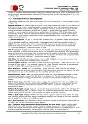
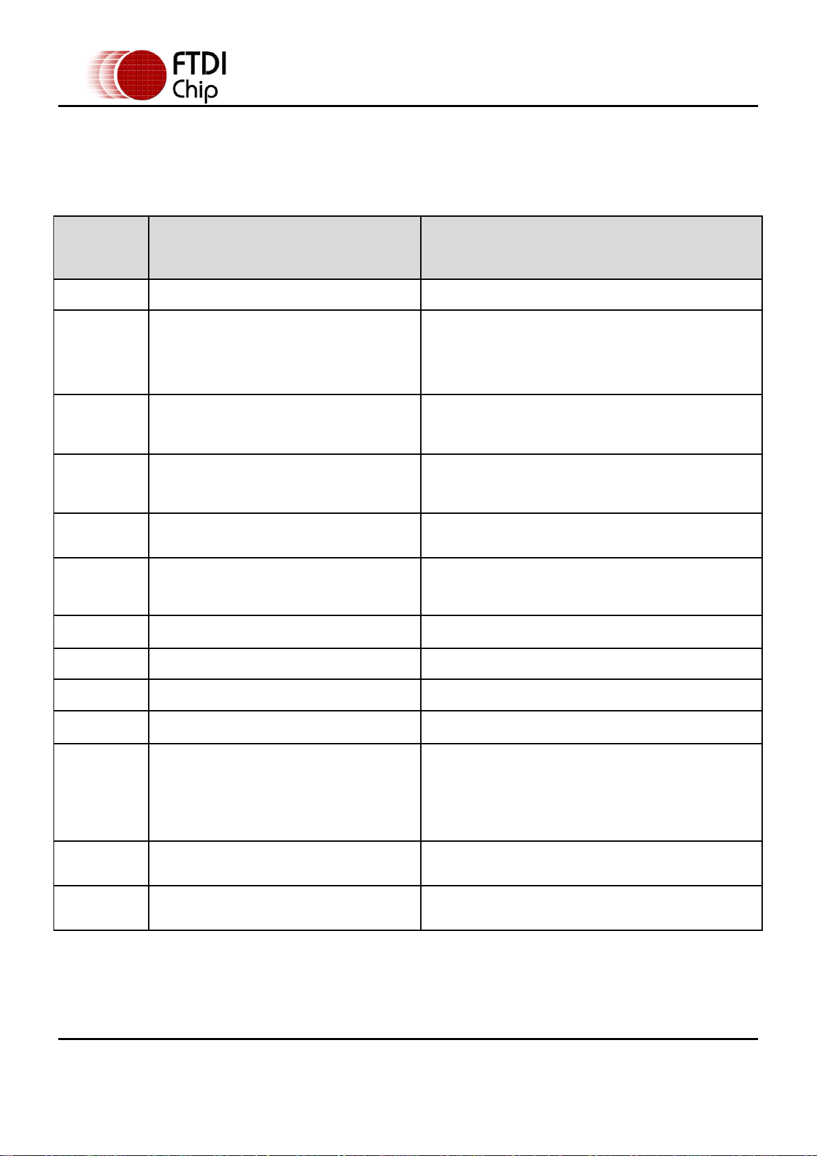
3.5 CBUS Signal Options
The following options can be configured on the CBUS I/O pins. CBUS signal options are common to both
package versions of the FT232R. These options can be configured in the internal EEPROM using the
software utility FT_PPROG or MPROG, which can be downloaded from the FTDI Utilities
(www.ftdichip.com). The default configuration is described in Section 8.
CBUS
Signal
Option
Available On CBUS Pin
Description
TXDEN
CBUS0, CBUS1, CBUS2, CBUS3, CBUS4
Enable transmit data for RS485
PWREN#
CBUS0, CBUS1, CBUS2, CBUS3, CBUS4
Output is low after the device has been configured by
USB, then high during USB suspend mode. This output can
be used to control power to external logic P-Channel logic
level MOSFET switch. Enable the interface pull-down
option when using the PWREN# in this way.*
TXLED#
CBUS0, CBUS1, CBUS2, CBUS3, CBUS4
Transmit data LED drive: Data from USB Host to
FT232R. Pulses low when transmitting data via USB. See
Section 7.5 for more details.
RXLED#
CBUS0, CBUS1, CBUS2, CBUS3, CBUS4
Receive data LED drive: Data from FT232R to USB Host.
Pulses low when receiving data via USB. See Section 7.5
for more details.
TX&RXLED#
CBUS0, CBUS1, CBUS2, CBUS3, CBUS4
LED drive – pulses low when transmitting or receiving data
via USB. See Section 7.5 for more details.
SLEEP#
CBUS0, CBUS1, CBUS2, CBUS3, CBUS4
Goes low during USB suspend mode. Typically used to
power down an external TTL to RS232 level converter IC
in USB to RS232 converter designs.
CLK48
CBUS0, CBUS1, CBUS2, CBUS3, CBUS4
48MHz ±0.7% Clock output. **
CLK24
CBUS0, CBUS1, CBUS2, CBUS3, CBUS4
24 MHz Clock output.**
CLK12
CBUS0, CBUS1, CBUS2, CBUS3, CBUS4
12 MHz Clock output.**
CLK6
CBUS0, CBUS1, CBUS2, CBUS3, CBUS4
6 MHz ±0.7% Clock output. **
CBitBangI/O
CBUS0, CBUS1, CBUS2, CBUS3
CBUS bit bang mode option. Allows up to 4 of the CBUS
pins to be used as general purpose I/O. Configured
individually for CBUS0, CBUS1, CBUS2 and CBUS3 in the
internal EEPROM. A separate application note, AN232R-01,
available from FTDI website (www.ftdichip.com) describes
in more detail how to use CBUS bit bang mode.
BitBangWRn
CBUS0, CBUS1, CBUS2, CBUS3
Synchronous and asynchronous bit bang mode WR#
strobe output.
BitBangRDn
CBUS0, CBUS1, CBUS2, CBUS3
Synchronous and asynchronous bit bang mode RD# strobe
output.
Table 3.9 CBUS Configuration Control
* PWREN# must be used with a 10kΩ resistor pull up.
**When in USB suspend mode the outputs clocks are also suspended.
器件 Datasheet 文档搜索
AiEMA 数据库涵盖高达 72,405,303 个元件的数据手册,每天更新 5,000 多个 PDF 文件
