Datasheet 搜索 > 接口芯片 > FTDI Chip(飞特帝亚) > FT232RQ-TRAY 数据手册 > FT232RQ-TRAY 数据手册 26/47 页
 器件3D模型
¥ 33.425
FT232RQ-TRAY 数据手册 - FTDI Chip(飞特帝亚)
制造商:
FTDI Chip(飞特帝亚)
分类:
接口芯片
封装:
QFN-32
Pictures:
3D模型
符号图
焊盘图
引脚图
产品图
页面导航:
引脚图在P7P10P13Hot
典型应用电路图在P2P28
原理图在P4P7
封装尺寸在P7P10P36P37
焊盘布局在P38P39
焊接温度在P39P40
功能描述在P14P15
技术参数、封装参数在P17
应用领域在P2P33
型号编号列表在P2
导航目录
FT232RQ-TRAY数据手册
Page:
of 47 Go
若手册格式错乱,请下载阅览PDF原文件
Copyright © 2010 Future Technology Devices International Limited 26
Document No.: FT_000053
FT232R USB UART IC Datasheet Version 2.11
Clearance No.: FTDI# 38
iii) One of the CBUS Pins should be configured as PWREN# in the internal FT232R EEPROM, and used
to switch the power supply to the external circuitry. This should be pulled high through a 10 kΩ
resistor.
iv) For USB high-power bus powered applications (one that consumes greater than 100mA, and up
to 500mA of current from the USB bus), the power consumption of the application must be set in
the Max Power field in the internal FT232R EEPROM. A high-power bus powered application uses
the descriptor in the internal FT232R EEPROM to inform the system of its power requirements.
v) PWREN# gets its VCC from VCCIO. For designs using 3V3 logic, ensure VCCIO is not powered
down using the external logic. In this case use the +3V3OUT.
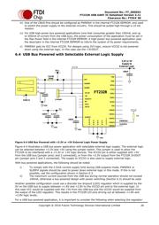
6.4 USB Bus Powered with Selectable External Logic Supply
FT232R
A
G
N
D
G
N
D
G
N
D
G
N
D
T
E
S
T
100nF
3V3OUT
VCCIO
NC
RESET#
NC
10nF
TXD
RXD
RTS#
CTS#
DTR#
DSR#
DCD#
RI#
CBUS0
CBUS3
CBUS2
CBUS1
USBDP
USBDM
VCC
1
2
3
4
5
OSCI
OSCO
CBUS4
Ferrite
Bead
+
SHIELD
GND
GND
GND
3.3V or 5V
Supply to
External Logic
100nF
+
100nF
Vcc
4.7uF
GND
1
Jumper
SLEEP#
PWREN#
2
3
Vcc
VCCIO
10K
VCCIO
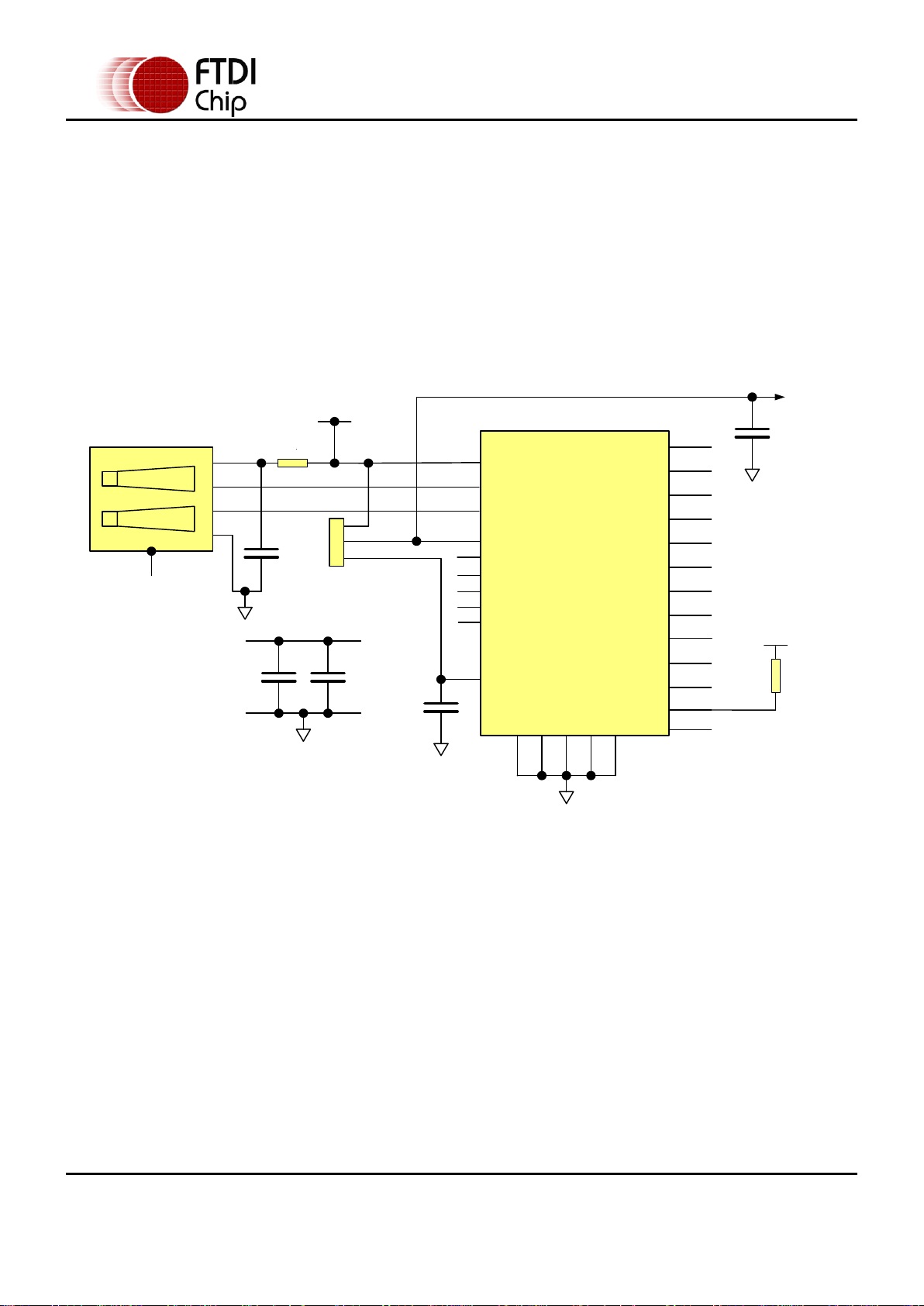
Figure 6.4 USB Bus Powered with +3.3V or +5V External Logic Power Supply
Figure 6.4 illustrates a USB bus power application with selectable external logic supply. The external logic
can be selected between +3.3V and +5V using the jumper switch. This jumper is used to allow the
FT232R to be interfaced with a +3.3V or +5V logic devices. The VCCIO pin is either supplied with +5V
from the USB bus (jumper pins1 and 2 connected), or from the +3.3V output from the FT232R 3V3OUT
pin (jumper pins 2 and 3 connected). The supply to VCCIO is also used to supply external logic.
With bus powered applications, the following should be noted:
i) To comply with the 2.5mA current supply limit during USB suspend mode, PWREN# or
SLEEP# signals should be used to power down external logic in this mode. If this is not
possible, use the configuration shown in Section 6.3.
ii) The maximum current sourced from the USB bus during normal operation should not exceed
100mA, otherwise a bus powered design with power switching (Section 6.3) should be used.
Another possible configuration could use a discrete low dropout (LDO) regulator which is supplied by the
5V on the USB bus to supply between +1.8V and +2.8V to the VCCIO pin and to the external logic. In
this case VCC would be supplied with the +5V from the USB bus and the VCCIO would be supplied from
the output of the LDO regulator. This results in the FT232R I/O pins driving out at between +1.8V and
+2.8V logic levels.
For a USB bus powered application, it is important to consider the following when selecting the regulator:
器件 Datasheet 文档搜索
AiEMA 数据库涵盖高达 72,405,303 个元件的数据手册,每天更新 5,000 多个 PDF 文件
