Datasheet 搜索 > CPLD芯片 > Lattice Semiconductor(莱迪思) > GAL16V8D-7LJ 数据手册 > GAL16V8D-7LJ 数据手册 3/26 页
 器件3D模型
¥ 0.452
GAL16V8D-7LJ 数据手册 - Lattice Semiconductor(莱迪思)
制造商:
Lattice Semiconductor(莱迪思)
分类:
CPLD芯片
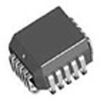
封装:
PLCC-20
Pictures:
3D模型
符号图
焊盘图
引脚图
产品图
页面导航:
引脚图在P3Hot
典型应用电路图在P8P10P12
原理图在P3P19
型号编码规则在P1P2P4
封装信息在P4P5
技术参数、封装参数在P4P5P6P7P8P9P10P11P12P14P15P16
应用领域在P3
导航目录
GAL16V8D-7LJ数据手册
Page:
of 26 Go
若手册格式错乱,请下载阅览PDF原文件
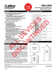
GAL16V8
High Performance E
2
CMOS PLD
Generic Array Logic™
1
2
20
I/CLKII
I
I
I
I
I
I GND
Vcc
I/O/Q I/O/Q
I/O/Q
I/O/Q
I/O/Q
I/O/Q
I/O/Q
I/O/Q
I/OE
4
6
8
9
11 13
14
16
18
1
10
11
20
I/CLK
I
I
I
I
I
I
I
I
GND
Vcc
I/O/Q
I/O/Q
I/O/Q
I/O/Q
I/O/Q
I/O/Q
I/O/Q
I/O/Q
I/OE
5
15
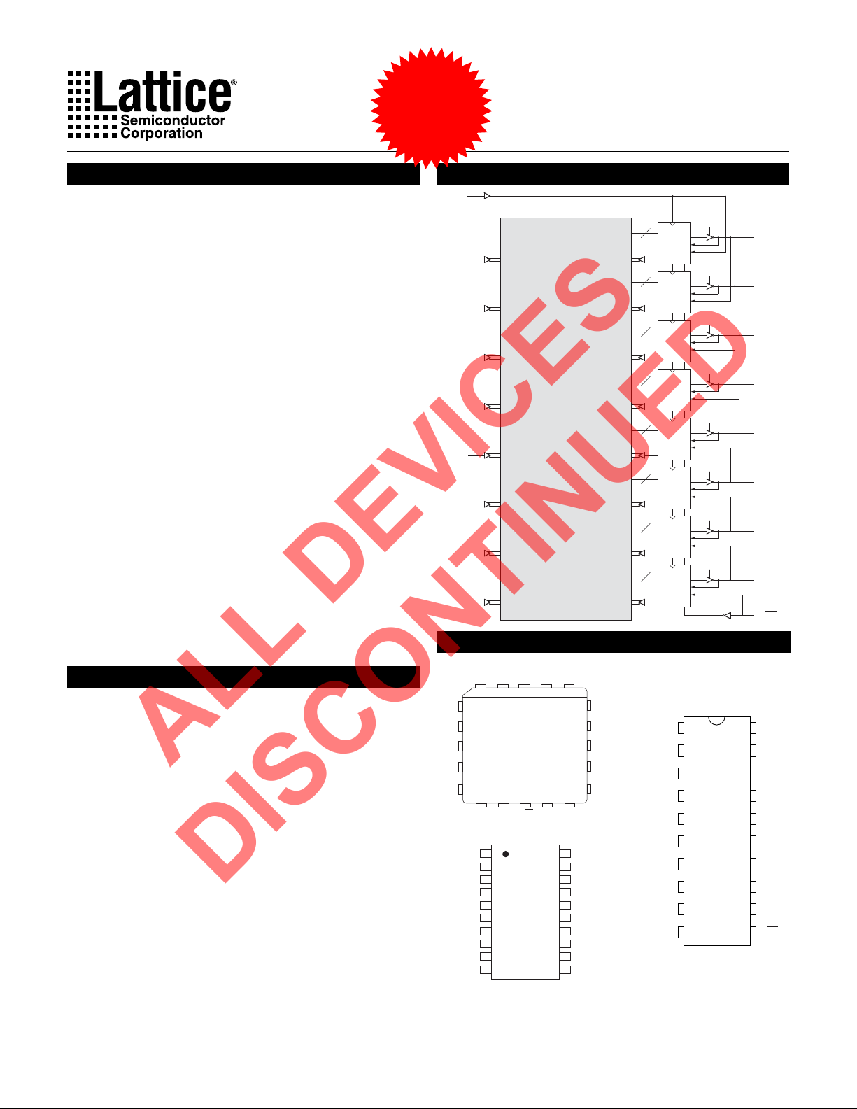
PLCC
GAL
16V8
DIP
GAL16V8
Top View
Copyright © 2006 Lattice Semiconductor Corp. All brand or product names are trademarks or registered trademarks of their respective holders. The specifications and information herein are subject
to change without notice.
LATTICE SEMICONDUCTOR CORP., 5555 Northeast Moore Ct., Hillsboro, Oregon 97124, U.S.A. August 2006
Tel. (503) 268-8000; 1-800-LATTICE; FAX (503) 268-8556; http://www.latticesemi.com
16v8_11
Features
• HIGH PERFORMANCE E
2
CMOS
®
TECHNOLOGY
— 3.5 ns Maximum Propagation Delay
— Fmax = 250 MHz
— 3.0 ns Maximum from Clock Input to Data Output
— UltraMOS
®
Advanced CMOS Technology
• 50% to 75% REDUCTION IN POWER FROM BIPOLAR
— 75mA Typ Icc on Low Power Device
— 45mA Typ Icc on Quarter Power Device
• ACTIVE PULL-UPS ON ALL PINS
•E
2
CELL TECHNOLOGY
— Reconfigurable Logic
— Reprogrammable Cells
— 100% Tested/100% Yields
— High Speed Electrical Erasure (<100ms)
— 20 Year Data Retention
• EIGHT OUTPUT LOGIC MACROCELLS
— Maximum Flexibility for Complex Logic Designs
— Programmable Output Polarity
— Also Emulates 20-pin PAL
®
Devices with Full
Function/Fuse Map/Parametric Compatibility
• PRELOAD AND POWER-ON RESET OF ALL REGISTERS
— 100% Functional Testability
• APPLICATIONS INCLUDE:
— DMA Control
— State Machine Control
— High Speed Graphics Processing
— Standard Logic Speed Upgrade
• ELECTRONIC SIGNATURE FOR IDENTIFICATION
• LEAD-FREE PACKAGE OPTIONS
Description
The GAL16V8, at 3.5 ns maximum propagation delay time, com-
bines a high performance CMOS process with Electrically Eras-
able (E
2
) floating gate technology to provide the highest speed
performance available in the PLD market. High speed erase times
(<100ms) allow the devices to be reprogrammed quickly and ef-
ficiently.
The generic architecture provides maximum design flexibility by
allowing the Output Logic Macrocell (OLMC) to be configured by
the user. An important subset of the many architecture configura-
tions possible with the GAL16V8 are the PAL
architectures listed
in the table of the macrocell description section. GAL16V8 devices
are capable of emulating any of these PAL architectures with full
function/fuse map/parametric compatibility.
Unique test circuitry and reprogrammable cells allow complete AC,
DC, and functional testing during manufacture. As a result, Lattice
Semiconductor delivers 100% field programmability and function-
ality of all GAL products. In addition, 100 erase/write cycles and
data retention in excess of 20 years are specified.
Functional Block Diagram
Pin Configuration
1
10
11
20I/CLK
I
I
I
I
I
I
I
I
GND
Vcc
I/O/Q
I/O/Q
I/O/Q
I/O/Q
I/O/Q
I/O/Q
I/O/Q
I/O/Q
I/OE
5
15
SOIC
GAL
16V8
Top
View
Lead-Free
Package
Options
Available!
I/CLK
I
I/O/Q
I
I/O/Q
I
I/O/Q
I
I/O/Q
I
I/O/Q
I
I/O/Q
I
I/O/Q
I
I/O/Q
CLK
8
8
8
8
8
8
8
8
OE
OLMC
OLMC
OLMC
OLMC
OLMC
OLMC
OLMC
OLMC
PROGRAMMABLE
AND-ARRAY
(64 X 32)
I/OE
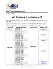
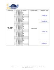
ALL DEVICES
DISCONTINUED
器件 Datasheet 文档搜索
AiEMA 数据库涵盖高达 72,405,303 个元件的数据手册,每天更新 5,000 多个 PDF 文件
