Datasheet 搜索 > 电压电平转换器 > NXP(恩智浦) > GTL2002DC,125 数据手册 > GTL2002DC,125 数据手册 1/27 页
 器件3D模型
¥ 2.674
GTL2002DC,125 数据手册 - NXP(恩智浦)
制造商:
NXP(恩智浦)
分类:
电压电平转换器
封装:
VSSOP-8
描述:
NXP### 并行输入/输出外设
Pictures:
3D模型
符号图
焊盘图
引脚图
产品图
页面导航:
导航目录
GTL2002DC,125数据手册
Page:
of 27 Go
若手册格式错乱,请下载阅览PDF原文件

1. General description
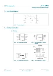
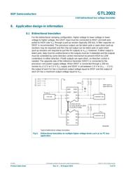
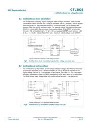
The Gunning Transceiver Logic - Transceiver Voltage Clamps (GTL-TVC) provide
high-speed voltage translation with low ON-state resistance and minimal propagation
delay. The GTL2002 provides 2 NMOS pass transistors (Sn and Dn) with a common gate
(GREF) and a reference transistor (SREF and DREF). The device allows bidirectional
voltage translations between 1.0 V and 5.0 V without use of a direction pin.
When the Sn or Dn port is LOW the clamp is in the ON-state and a low resistance
connection exists between the Sn and Dn ports. Assuming the higher voltage is on the Dn
port, when the Dn port is HIGH, the voltage on the Sn port is limited to the voltage set by
the reference transistor (SREF). When the Sn port is HIGH, the Dn port is pulled to V
CC
by
the pull-up resistors. This functionality allows a seamless translation between higher and
lower voltages selected by the user, without the need for directional control.
All transistors have the same electrical characteristics and there is minimal deviation from
one output to another in voltage or propagation delay. This is a benefit over discrete
transistor voltage translation solutions, since the fabrication of the transistors is
symmetrical. Because all transistors in the device are identical, SREF and DREF can be
located on any of the other two matched Sn/Dn transistors, allowing for easier board
layout. The translator's transistors provide excellent ESD protection to lower voltage
devices and at the same time protect less ESD-resistant devices.
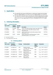
2. Features and benefits
2-bit bidirectional low voltage translator
Allows voltage level translation between 1.0V, 1.2V, 1.5V, 1.8V, 2.5V, 3.3V and 5V
buses, which allows direct interface with GTL, GTL+, LVTTL/TTL and 5 V CMOS
levels
Provides bidirectional voltage translation with no direction pin
Low 6.5 ON-state resistance (R
on
) between input and output pins (Sn/Dn)
Supports hot insertion
No power supply required; will not latch up
5 V tolerant inputs
Low standby current
Flow-through pinout for ease of printed-circuit board trace routing
ESD protection exceeds 2000 V HBM per JESD22-A114 and 1000 V CDM per
JESD22-C101
Packages offered: SO8, TSSOP8 (MSOP8), VSSOP8, XQFN8
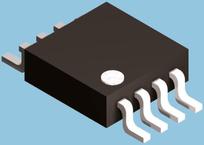
GTL2002
2-bit bidirectional low voltage translator
Rev. 8 — 19 August 2013 Product data sheet
器件 Datasheet 文档搜索
AiEMA 数据库涵盖高达 72,405,303 个元件的数据手册,每天更新 5,000 多个 PDF 文件
