Datasheet 搜索 > 模拟开关芯片 > NXP(恩智浦) > HEF4053BT 数据手册 > HEF4053BT 数据手册 4/20 页
 器件3D模型
¥ 3.421
HEF4053BT 数据手册 - NXP(恩智浦)
制造商:
NXP(恩智浦)
分类:
模拟开关芯片
封装:
SOIC
描述:
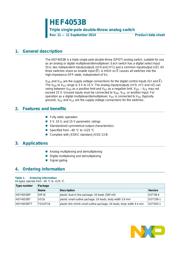
NXP HEF4053BT 模拟开关, SPDT, 3 放大器, 60 ohm, 4.5V 至 15.5V, SOIC, 16 引脚
Pictures:
3D模型
符号图
焊盘图
引脚图
产品图
页面导航:
导航目录
HEF4053BT数据手册
Page:
of 20 Go
若手册格式错乱,请下载阅览PDF原文件
HEF4053B All information provided in this document is subject to legal disclaimers. © NXP Semiconductors N.V. 2014. All rights reserved.
Product data sheet Rev. 11 — 11 September 2014 4 of 20
NXP Semiconductors
HEF4053B
Triple single-pole double-throw analog switch
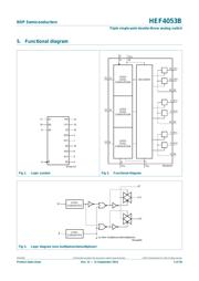
7. Functional description
[1] H = HIGH voltage level; L = LOW voltage level; X = don’t care.
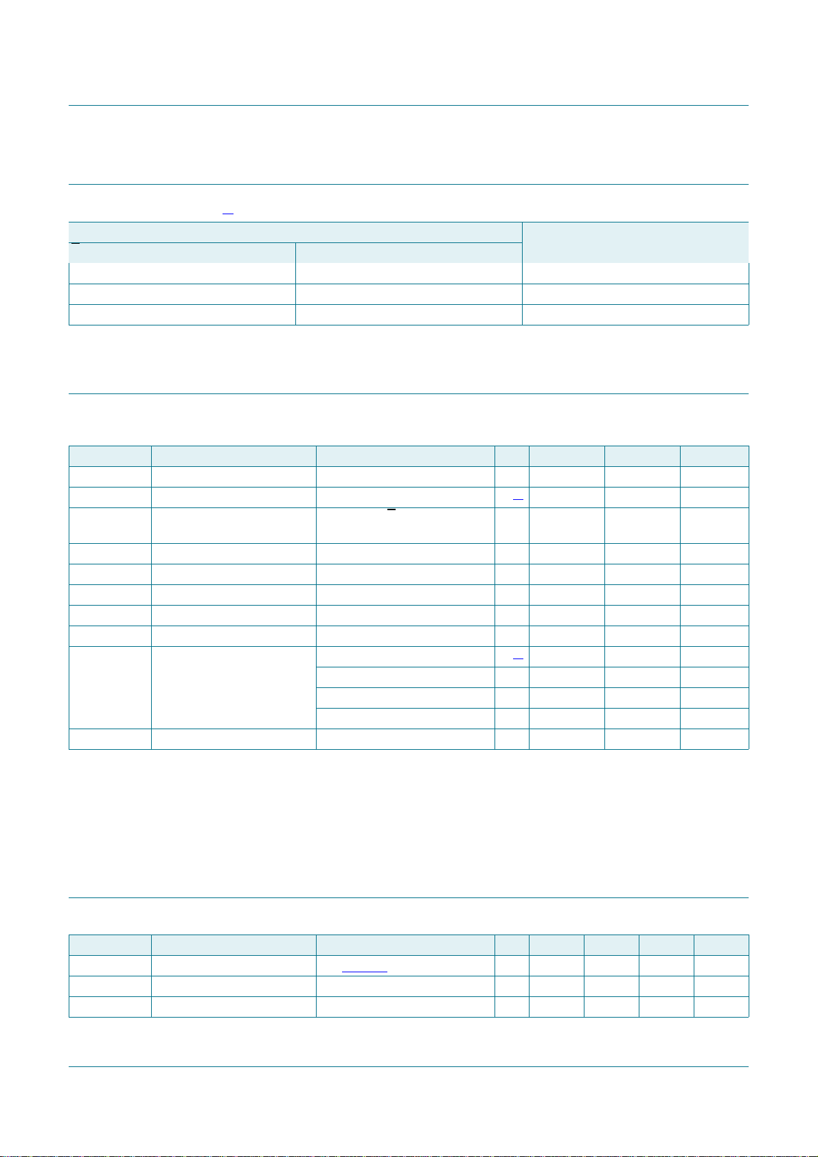
8. Limiting values
[1] To avoid drawing V
DD
current out of terminal Z, when switch current flows into terminals Y, the voltage drop across the bidirectional
switch must not exceed 0.4 V. If the switch current flows into terminal Z, no V
DD
current will flow out of terminals Y, and in this case there
is no limit for the voltage drop across the switch, but the voltages at Y and Z may not exceed V
DD
or V
EE
.
[2] For DIP16 package: P
tot
derates linearly with 12 mW/K above 70 C.
For SO16 package: P
tot
derates linearly with 8 mW/K above 70 C.
For TSSOP16 package: P
tot
derates linearly with 5.5 mW/K above 60 C.
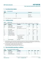
9. Recommended operating conditions
Table 3. Function table
[1]
Inputs Channel on
E Sn
LLnY0 to nZ
L H nY1 to nZ
H X switches OFF
Table 4. Limiting values
In accordance with the Absolute Maximum Rating System (IEC 60134). Voltages are referenced to V
SS
= 0 V (ground).
Symbol Parameter Conditions Min Max Unit
V
DD
supply voltage 0.5 +18 V
V
EE
supply voltage referenced to V
DD
[1]
18 +0.5 V
I
IK
input clamping current pins Sn and E;
V
I
< 0.5 V or V
I
>V
DD
+ 0.5 V
- 10 mA
V
I
input voltage 0.5 V
DD
+ 0.5 V
I
I/O
input/output current - 10 mA
I
DD
supply current - 50 mA
T
stg
storage temperature 65 +150 C
T
amb
ambient temperature 40 +125 C
P
tot
total power dissipation T
amb
= 40 C to +125 C
[2]
DIP16 package - 750 mW
SO16 package - 500 mW
TSSOP16 package - 500 mW
P power dissipation per output - 100 mW
Table 5. Recommended operating conditions
Symbol Parameter Conditions Min Typ Max Unit
V
DD
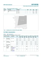
supply voltage see Figure 7 3- 15V
V
I
input voltage 0 - V
DD
V
T
amb
ambient temperature in free air 40 - +125 C
器件 Datasheet 文档搜索
AiEMA 数据库涵盖高达 72,405,303 个元件的数据手册,每天更新 5,000 多个 PDF 文件
