Datasheet 搜索 > FET驱动器 > Infineon(英飞凌) > IR2233JPBF 数据手册 > IR2233JPBF 数据手册 2/27 页
 器件3D模型
¥ 10.851
IR2233JPBF 数据手册 - Infineon(英飞凌)
制造商:
Infineon(英飞凌)
分类:
FET驱动器
封装:
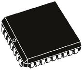
PLCC-44
描述:
INFINEON IR2233JPBF 功率驱动器, 3相桥接, 10V-20V电源, 500mA输出, 700ns延迟, LCC-44
Pictures:
3D模型
符号图
焊盘图
引脚图
产品图
页面导航:
导航目录
IR2233JPBF数据手册
Page:
of 27 Go
若手册格式错乱,请下载阅览PDF原文件
IR2133/IR2135/IR2233
/
IR2235(J
&
S
) & (PbF)
2 www.irf.com
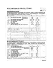
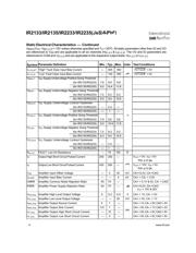
Absolute Maximum Ratings
Absolute Maximum Ratings indicate sustained limits beyond which damage to the device may occur. All volt-
age parameters are absolute voltages referenced to COM. The Thermal Resistance and Power Dissipation
ratings are measured under board mounted and still air conditions.
Recommended Operating Conditions
The input/output logic timing diagram is shown in figure 1. For proper operation the device should be used within the
recommended conditions. All voltage parameters are absolute voltages referenced to COM. The V
S
offset rating is
tested with all supplies biased at 15V differential.
Note 1:
Logic operational for V
S
of COM - 5V to COM + 600V/1200V. Logic state held for V
S
of COM -5V to COM -V
BS
. (Please refer to the Design Tip
DT97-3 for more details).
Note 2: All input pins, op amp input and output pins are internally clamped with a 5.2V zener diode.
Symbol Definition Min. Max. Units
V
B1,2,3
High side floating supply voltage (IR2133/IR2135) -0.3 625
(IR2233/IR2235) -0.3 1225
V
S1,2,3
High side floating supply offset voltage V
B1,2,3
- 25 V
B1,2,3
+ 0.3
V
HO1,2,3
High side floating output voltage V
S1,2,3
- 0.3 V
B1,2,3
+ 0.3
V
CC
Fixed supply voltage -0.3 25
V
SS
Logic ground V
CC
- 25 V
CC
+ 0.3
V
LO1,2,3
Low side output voltage -0.3 V
CC
+ 0.3
V
IN
Logic input voltage (HIN, LIN, ITRIP, SD & FLT-CLR) V
SS
- 0.3 (V
SS
+ 15) or
(V
CC
+ 0.3)
whichever is
lower
V
IN,AMP
Op amp input voltage (CA+ & CA-) V
SS
- 0.3 V
CC
+ 0.3
V
OUT,AMP
Op amp output voltage (CAO) V
SS
- 0.3 V
CC
+ 0.3
V
FLT
FAULT
output voltage
V
SS
- 0.3 V
CC
+ 0.3
dV
S
/dt Allowable offset supply voltage transient — 50
P
D
Package power dissipation @ T
A
≤ 25ºC (28 Lead PDIP) — 1.5
(28 Lead SOIC) — 1.6
(44 lead PLCC) — 2.0
Rth
JA
Thermal resistance, junction to ambient (28 Lead PDIP) — 83
(28 Lead SOIC) — 78
(44 lead PLCC) — 63
T
J
Junction temperature — 125
T
S
Storage temperature -55 150
T
L
Lead temperature (soldering, 10 seconds — 300
ºC
W
V
B1,2,3
High side floating supply voltage V
S1,2,3
+ 10/12 V
S1,2,3
+ 20
V
S1,2,3
High side floating supply offset voltage (IR2133/IR2135) Note 1 600
(IR2233/IR2235) Note 1 1200
V
HO1,2,3
High side floating output voltage V
S1,2,3
V
B1,2,3
V
CC
Fixed supply voltage 10 or 12 20
V
SS
Low side driver return -5 5
V
LO1,2,3
Low side output voltage 0 V
CC
V
IN
Logic input voltage (HIN, LIN, ITRIP, SD & FLT-CLR) V
SS
V
SS
+ 5
V
IN,AMP
Op amp input voltage (CA+ & CA-) V
SS
V
SS
+ 5
V
OUT,AMP
Op amp output voltage (CAO) V
SS
V
SS
+ 5
V
FLT
FAULT
output voltage
V
SS
V
CC
V
Symbol Parameter Definition Min. Max. Units
V/ns
V
ºC/W
器件 Datasheet 文档搜索
AiEMA 数据库涵盖高达 72,405,303 个元件的数据手册,每天更新 5,000 多个 PDF 文件
