Datasheet 搜索 > MOS管 > VISHAY(威世) > IRF9Z14STRLPBF 数据手册 > IRF9Z14STRLPBF 数据手册 1/10 页
¥ 3.124
IRF9Z14STRLPBF 数据手册 - VISHAY(威世)
制造商:
VISHAY(威世)
分类:
MOS管
封装:
TO-252-3
描述:
功率MOSFET Power MOSFET
Pictures:
3D模型
符号图
焊盘图
引脚图
产品图
页面导航:
封装尺寸在P8
型号编码规则在P1
功能描述在P1P10
技术参数、封装参数在P1P2P10
导航目录
IRF9Z14STRLPBF数据手册
Page:
of 10 Go
若手册格式错乱,请下载阅览PDF原文件
Document Number: 91089
www.vishay.com
S11-1052-Rev. C, 30-May-11 1
This document is subject to change without notice.
THE PRODUCTS DESCRIBED HEREIN AND THIS DOCUMENT ARE SUBJECT TO SPECIFIC DISCLAIMERS, SET FORTH AT
www.vishay.com/doc?91000
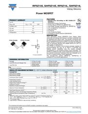
Power MOSFET
IRF9Z14S, SiHF9Z14S, IRF9Z14L, SiHF9Z14L
Vishay Siliconix
FEATURES
• Halogen-free According to IEC 61249-2-21
Definition
• Advanced Process Technology
• Surface Mount (IRF9Z14S, SiHF9Z14S)
•
Low-Profile Through-Hole (IRF9Z14L, SiHF9Z14L)
• 175 °C Operating Temperature
•Fast Switching
• P-Channel
• Fully Avalanche Rated
• Compliant to RoHS Directive 2002/95/EC
DESCRIPTION
Third generation Power MOSFETs from Vishay utilize
advanced processing techniques to achieve extremely low
on-resistance per silicon area. This benefit, combined with
the fast switching speed and ruggedized device design that
Power MOSFETs are well known for, provides the designer
with an extremely efficient and reliable device for use in a
wide variety of applications.
The D
2
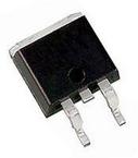
PAK is a surface mount power package capable of
accommodating die size up to HEX-4. It provides the
highest power capability and the lowest possible
on-resistance in any existing surface mount package. The
D
2
PAK is suitable for high current applications because of is
low internal connection resistance and can dissipate up to
2.0 W in a typical surface mount application.
The through-hole version (IRF9Z14L, SiHF9Z14L) is
available for low-profile applications.
Note
a. See device orientation.
Notes
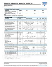
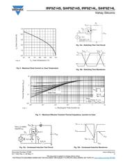
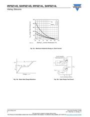
a. Repetitive rating; pulse width limited by maximum junction temperature (see fig. 11).
b. V
DD
= - 25 V, starting T
J
= 25 °C, L = 3.6 mH, R
g
= 25 , I
AS
= - 6.7 A (see fig. 12).
c. I
SD
- 6.7 A, dI/dt 90 A/μs, V
DD
V
DS
, T
J
175 °C.
d. 1.6 mm from case.
e. Uses IRF9Z14, SiHF9Z14 data and test conditions.
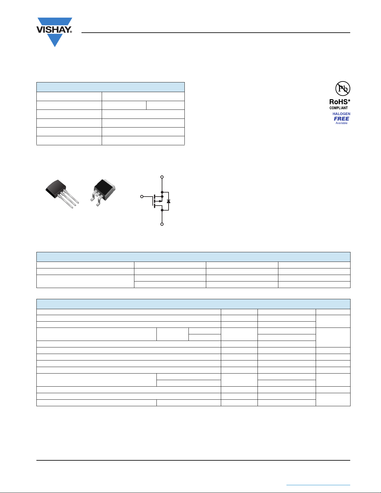
PRODUCT SUMMARY
V
DS
(V) - 60
R
DS(on)
()V
GS
= - 10 V 0.50
Q
g
(Max.) (nC) 12
Q
gs
(nC) 3.8
Q
gd
(nC) 5.1
Configuration Single
S
G
D
P-Channel MOSFET
D
2
PAK (TO-263)
G
D
S
I
2
PAK (TO-262)
G
D
S
ORDERING INFORMATION
Package D
2
PAK (TO-263) D
2
PAK (TO-263) I
2
PAK (TO-262)
Lead (Pb)-free and Halogen-free SiHF9Z14S-GE3 SiHF9Z14STRL-GE3
a
SiHF9Z14L-GE3
Lead (Pb)-free
IRF9Z14SPbF IRF9Z14STRLPbF
a
IRF9Z14LPbF
SiHF9Z14S-E3 SiHF9Z14STL-E3
a
SiHF9Z14L-E3
ABSOLUTE MAXIMUM RATINGS (T
C
= 25 °C, unless otherwise noted)
PARAMETER SYMBOL LIMIT UNIT
Drain-Source Voltage V
DS
- 60
V
Gate-Source Voltage V
GS
± 20
Continuous Drain Current
e
V
GS
at - 10 V
T
C
= 25 °C
I
D
- 6.7
A
T
C
= 100 °C - 4.7
Pulsed Drain Current
a, e
I
DM
- 27
Linear Derating Factor 0.29 W/°C
Single Pulse Avalanche Energy
b, e
E
AS
140 mJ
Avalanche Current
a
I
AR
- 6.7 A
Repetiitive Avalanche Energy
a
E
AR
4.3 mJ
Maximum Power Dissipation
T
C
= 25 °C
P
D
43
W
T
A
= 25 °C 3.7
Peak Diode Recovery dV/dt
c, e
dV/dt - 4.5 V/ns
Operating Junction and Storage Temperature Range T
J
, T
stg
- 55 to + 175
°C
Soldering Recommendations (Peak Temperature) for 10 s 300
d
* Pb containing terminations are not RoHS compliant, exemptions may apply
器件 Datasheet 文档搜索
AiEMA 数据库涵盖高达 72,405,303 个元件的数据手册,每天更新 5,000 多个 PDF 文件

