Datasheet 搜索 > MOS管 > Vishay Siliconix > IRFR110 数据手册 > IRFR110 数据手册 1/11 页

¥ 1.519
IRFR110 数据手册 - Vishay Siliconix
制造商:
Vishay Siliconix
分类:
MOS管
封装:
TO-252-3
Pictures:
3D模型
符号图
焊盘图
引脚图
产品图
页面导航:
导航目录
IRFR110数据手册
Page:
of 11 Go
若手册格式错乱,请下载阅览PDF原文件
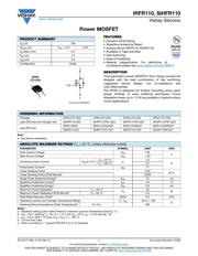
IRFR110, SiHFR110
www.vishay.com
Vishay Siliconix
S13-0171-Rev. F, 04-Feb-13
1
Document Number: 91265
For technical questions, contact: hvm@vishay.com
THIS DOCUMENT IS SUBJECT TO CHANGE WITHOUT NOTICE. THE PRODUCTS DESCRIBED HEREIN AND THIS DOCUMENT
ARE SUBJECT TO SPECIFIC DISCLAIMERS, SET FORTH AT www.vishay.com/doc?91000
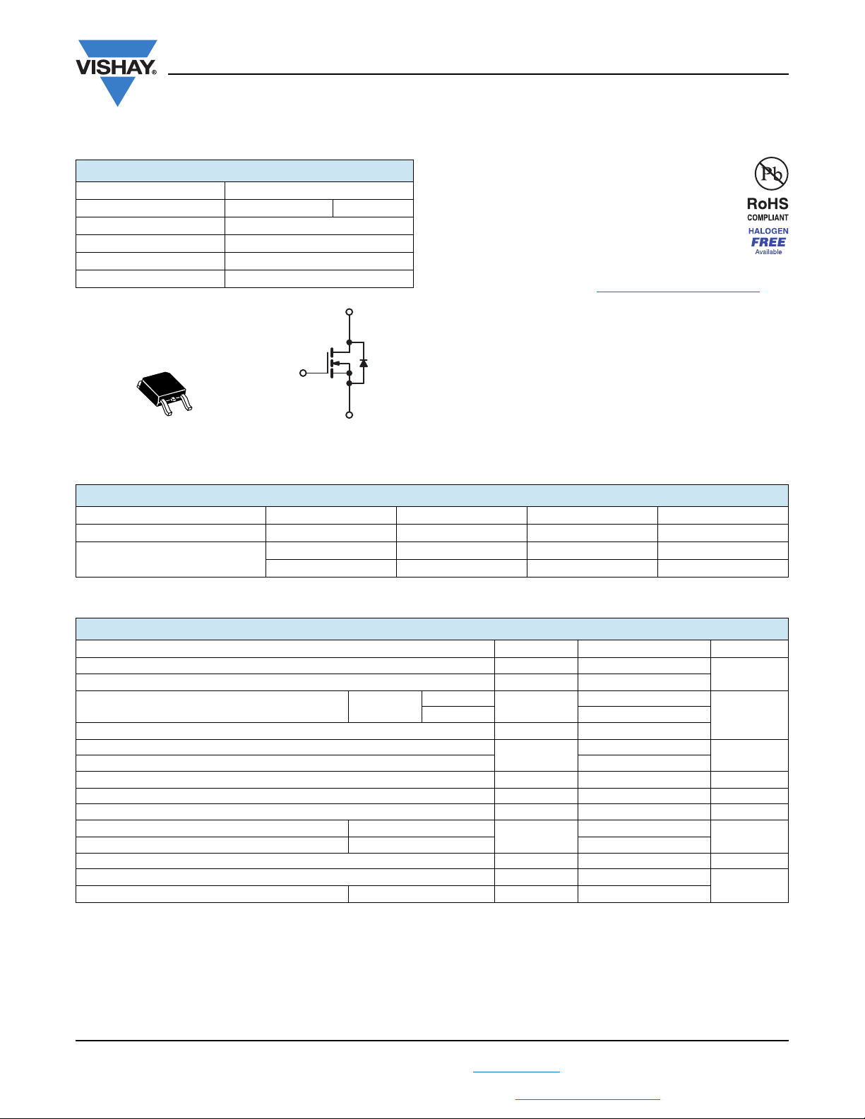
Power MOSFET
FEATURES
• Dynamic dV/dt Rating
• Repetitive Avalanche Rated
• Surface Mount (IRFR110, SiHFR110)
• Available in Tape and Reel
• Fast Switching
• Ease of Paralleling
• Material categorization: For definitions of
compliance please see www.vishay.com/doc?99912
DESCRIPTION
Third generation power MOSFETs from Vishay provide the
designer with the best combination of fast switching,
ruggedized device design, low on-resistance and
cost-effectiveness.
The DPAK is designed for surface mounting using vapor
phase, infrared, or wave soldering techniques. Power
dissipation levels up to 1.5 W are possible in typical surface
mount applications.
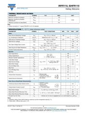
Note
a. See device orientation.
Notes
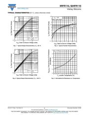
a. Repetitive rating; pulse width limited by maximum junction temperature (see fig. 11).
b. V
DD
= 25 V, starting T
J
= 25 °C, L = 8.1 mH, R
g
= 25 , I
AS
= 4.3 A (see fig. 12).
c. I
SD
5.6 A, dI/dt 75 A/μs, V
DD
V
DS
, T
J
150 °C.
d. 1.6 mm from case.
e. When mounted on 1" square PCB (FR-4 or G-10 material).
PRODUCT SUMMARY
V
DS
(V) 100
R
DS(on)
()V
GS
= 10 V 0.54
Q
g
(Max.) (nC) 8.3
Q
gs
(nC) 2.3
Q
gd
(nC) 3.8
Configuration Single
N-Channel MOSFET
G
D
S
DPAK
(TO-252)
S
D
G
ORDERING INFORMATION
Package DPAK (TO-252) DPAK (TO-252) DPAK (TO-252) DPAK (TO-252)
Lead (Pb)-free and Halogen-free SiHFR110-GE3 SiHFR110TRL-GE3 SiHFR110TR-GE3 SiHFR110TRR-GE3
Lead (Pb)-free
IRFR110PbF IRFR110TRLPbF
a
IRFR110TRPbF
a
IRFR110TRRPbF
a
SiHFR110-E3 SiHFR110TL-E3
a
SiHFR110T-E3
a
SiHFR110TR-E3
a
ABSOLUTE MAXIMUM RATINGS (T
C
= 25 °C, unless otherwise noted)
PARAMETER SYMBOL LIMIT UNIT
Drain-Source Voltage V
DS
100
V
Gate-Source Voltage V
GS
± 20
Continuous Drain Current V
GS
at 10 V
T
C
= 25 °C
I
D
4.3
AT
C
= 100 °C 2.7
Pulsed Drain Current
a
I
DM
17
Linear Derating Factor 0.20
W/°C
Linear Derating Factor (PCB Mount)
e
0.020
Single Pulse Avalanche Energy
b
E
AS
75 mJ
Repetitive Avalanche Current
a
I
AR
4.3 A
Repetitive Avalanche Energy
a
E
AR
2.5 mJ
Maximum Power Dissipation T
C
= 25 °C
P
D
25
W
Maximum Power Dissipation (PCB Mount)
e
T
A
= 25 °C 2.5
Peak Diode Recovery dV/dt
c
dV/dt 5.5 V/ns
Operating Junction and Storage Temperature Range T
J
, T
stg
- 55 to + 150
°C
Soldering Recommendations (Peak Temperature)
d
for 10 s 260
器件 Datasheet 文档搜索
AiEMA 数据库涵盖高达 72,405,303 个元件的数据手册,每天更新 5,000 多个 PDF 文件
