Datasheet 搜索 > Infineon(英飞凌) > IRFR3806 数据手册 > IRFR3806 数据手册 2/10 页


¥ 1.324
IRFR3806 数据手册 - Infineon(英飞凌)
制造商:
Infineon(英飞凌)
封装:
TO-252
Pictures:
3D模型
符号图
焊盘图
引脚图
产品图
页面导航:
封装尺寸在P8P9
标记信息在P8P9
技术参数、封装参数在P1
应用领域在P1
导航目录
IRFR3806数据手册
Page:
of 10 Go
若手册格式错乱,请下载阅览PDF原文件
IRFR/U3806PbF
2 www.irf.com
Notes:
Repetitive rating; pulse width limited by max. junction
temperature.
Limited by T
Jmax
, starting T
J
= 25°C, L = 0.23mH
R
G
= 25Ω, I
AS
= 25A, V
GS
=10V. Part not recommended for
use above this value.
I
SD
≤ 25A, di/dt ≤ 1580A/µs, V
DD
≤ V
(BR)DSS
, T
J
≤ 175°C.
Pulse width ≤ 400µs; duty cycle ≤ 2%.
S
D
G
C
oss
eff. (TR) is a fixed capacitance that gives the same charging time
as C
oss
while V
DS
is rising from 0 to 80% V
DSS
.
C
oss
eff. (ER) is a fixed capacitance that gives the same energy as
C
oss
while V
DS
is rising from 0 to 80% V
DSS
.
When mounted on 1" square PCB (FR-4 or G-10 Material). For recom
mended footprint and soldering techniques refer to application note #AN-994.
R
θ
is measured at T
J
approximately 90°C.
Static @ T
J
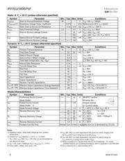
= 25°C (unless otherwise specified)
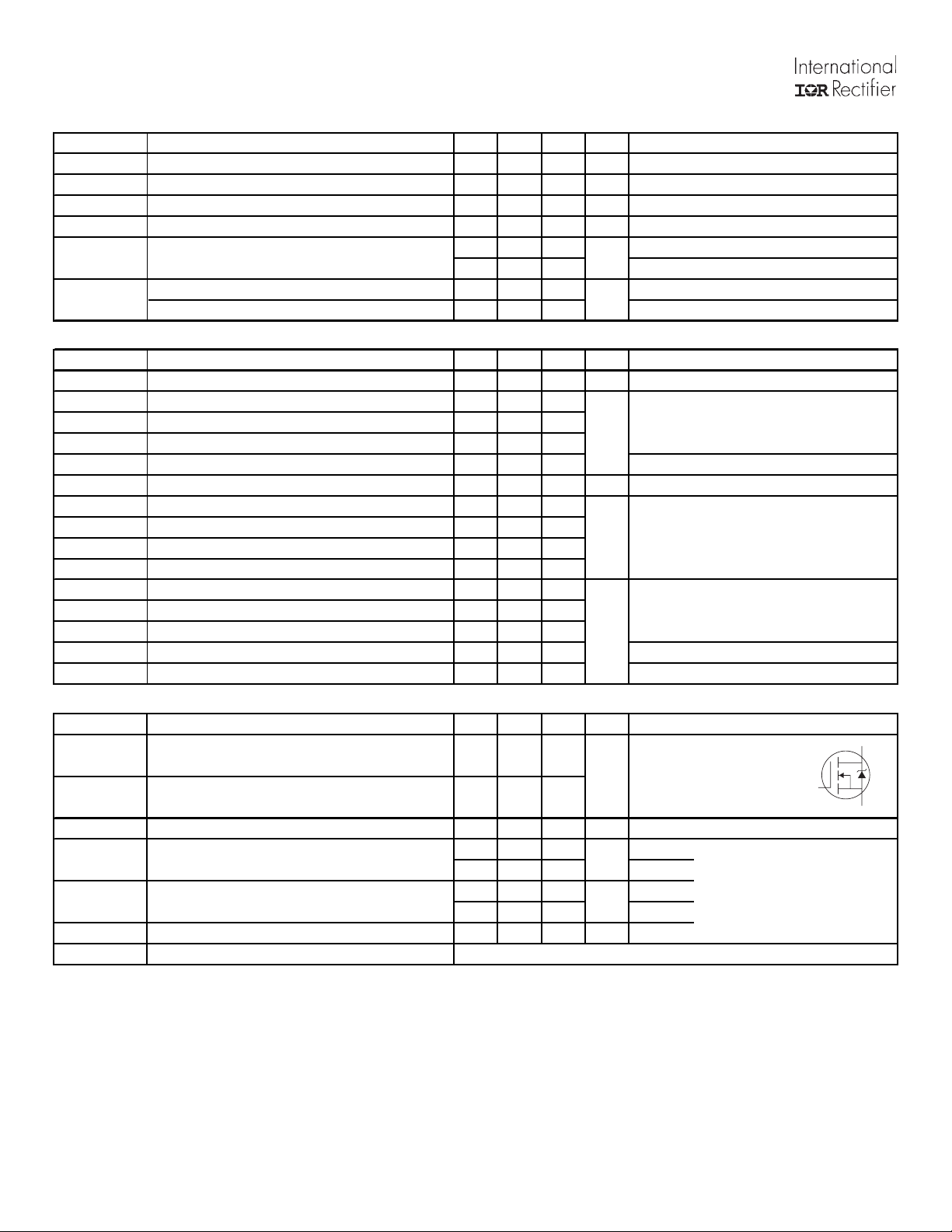
Symbol Parameter Min. Typ. Max. Units
V
(BR)DSS
Drain-to-Source Breakdown Voltage 60 ––– ––– V
∆V
(BR)DSS
/
∆T
J
Breakdown Voltage Temp. Coefficient ––– 0.075 ––– V/°C
R
DS(on)
Static Drain-to-Source On-Resistance ––– 12.6 15.8
mΩ
V
GS(th)
Gate Threshold Voltage 2.0 ––– 4.0 V
I
DSS
Drain-to-Source Leakage Current ––– ––– 20 µA
––– ––– 250
I
GSS
Gate-to-Source Forward Leakage ––– ––– 100 nA
Gate-to-Source Reverse Leakage ––– ––– -100
Dynamic @ T
J
= 25°C (unless otherwise specified)
Symbol Parameter Min. Typ. Max. Units
gfs Forward Transconductance 41 ––– ––– S
Q
g
Total Gate Charge ––– 22 30 nC
Q
gs
Gate-to-Source Charge ––– 5.0 –––
Q
gd
Gate-to-Drain ("Miller") Charge ––– 6.3 –––
Q
sync
Total Gate Charge Sync. (Q
g
- Q
gd
)
––– 28.3 –––
R
G(int)
Internal Gate Resistance
–––
0.79 –––
Ω
t
d(on)
Turn-On Delay Time ––– 6.3 ––– ns
t
r
Rise Time ––– 40 –––
t
d(off)
Turn-Off Delay Time ––– 49 –––
t
f
Fall Time ––– 47 –––
C
iss
Input Capacitance ––– 1150 –––
C
oss
Output Capacitance ––– 130 –––
C
rss
Reverse Transfer Capacitance ––– 67 ––– pF
C
oss
eff. (ER)
Effective Output Capacitance (Energy Related)
h
––– 190 –––
C
oss
eff. (TR)
Effective Output Capacitance (Time Related)
g
––– 230 –––
Diode Characteristics
Symbol Parameter Min. Typ. Max. Units
I
S
Continuous Source Current ––– –––
43
A
(Body Diode)
I
SM
Pulsed Source Current ––– ––– 170
(Body Diode)
c
V
SD
Diode Forward Voltage ––– ––– 1.3 V
t
rr
Reverse Recovery Time ––– 22 33 ns
T
J
= 25°C V
R
= 51V,
––– 26 39
T
J
= 125°C I
F
= 25A
Q
rr
Reverse Recovery Charge ––– 17 26 nC
T
J
= 25°C
di/dt = 100A/µs
f
––– 24 36
T
J
= 125°C
I
RRM
Reverse Recovery Current ––– 1.4 ––– A
T
J
= 25°C
t
on
Forward Turn-On Time Intrinsic turn-on time is negligible (turn-on is dominated by LS+LD)
Conditions
V
DS
= 10V, I
D
= 25A
I
D
= 25A
V
GS
= 20V
V
GS
= -20V
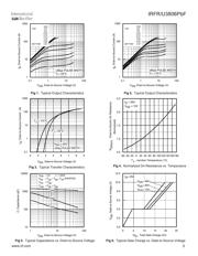
MOSFET symbol
showing the
V
DS
= 30V
Conditions
V
GS
= 10V
f
V
GS
= 0V
V
DS
= 50V
ƒ = 1.0MHz
V
GS
= 0V, V
DS
= 0V to 60V
h
V
GS
= 0V, V
DS
= 0V to 60V
g
T
J
= 25°C, I
S
= 25A, V
GS
= 0V
f
integral reverse
p-n junction diode.
Conditions
V
GS
= 0V, I
D
= 250µA
Reference to 25°C, I
D
= 5mA
c
V
GS
= 10V, I
D
= 25A
f
V
DS
= V
GS
, I
D
= 50µA
V
DS
= 60V, V
GS
= 0V
V
DS
= 48V, V
GS
= 0V, T
J
= 125°C
I
D
= 25A
R
G
= 20Ω
V
GS
= 10V
f
V
DD
= 39V
I
D
= 25A, V
DS
=0V, V
GS
= 10V
器件 Datasheet 文档搜索
AiEMA 数据库涵盖高达 72,405,303 个元件的数据手册,每天更新 5,000 多个 PDF 文件
