Datasheet 搜索 > MOS管 > Infineon(英飞凌) > IRFS3004PBF 数据手册 > IRFS3004PBF 数据手册 2/11 页

¥ 22.094
IRFS3004PBF 数据手册 - Infineon(英飞凌)
制造商:
Infineon(英飞凌)
分类:
MOS管
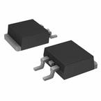
封装:
TO-263-3
描述:
INFINEON IRFS3004PBF 晶体管, MOSFET, N沟道, 195 A, 40 V, 0.0014 ohm, 10 V, 4 V
Pictures:
3D模型
符号图
焊盘图
引脚图
产品图
页面导航:
封装尺寸在P8P9P10
标记信息在P8P9P10
技术参数、封装参数在P1
应用领域在P1
导航目录
IRFS3004PBF数据手册
Page:
of 11 Go
若手册格式错乱,请下载阅览PDF原文件
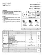
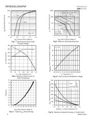
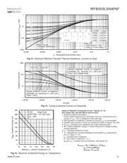
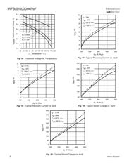
IRFB/S/SL3004PbF
2 www.irf.com
Notes:
Calculated continuous current based on maximum allowable junction
temperature. Bond wire current limit is 195A. Note that current
limitations arising from heating of the device leads may occur with
some lead mounting arrangements. (Refer to AN-1140)
Repetitive rating; pulse width limited by max. junction
temperature.
Limited by T
Jmax
, starting T
J
= 25°C, L = 0.016mH
R
G
= 25Ω, I
AS
= 195A, V
GS
=10V. Part not recommended for use
above this value .
S
D
G
I
SD
≤ 195A, di/dt ≤ 930A/µs, V
DD
≤ V
(BR)DSS
, T
J
≤ 175°C.
Pulse width ≤ 400µs; duty cycle ≤ 2%.
C
oss
eff. (TR) is a fixed capacitance that gives the same charging time
as C
oss
while V
DS
is rising from 0 to 80% V
DSS
.
C
oss
eff. (ER) is a fixed capacitance that gives the same energy as
C
oss
while V
DS
is rising from 0 to 80% V
DSS
.
When mounted on 1" square PCB (FR-4 or G-10 Material). For recom
mended footprint and soldering techniques refer to application note #AN-994.
R
θ
is measured at T
J
approximately 90°C.
R
θJC
value shown is at time zero.
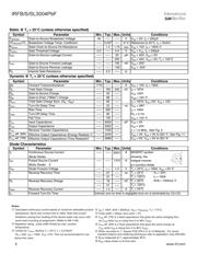
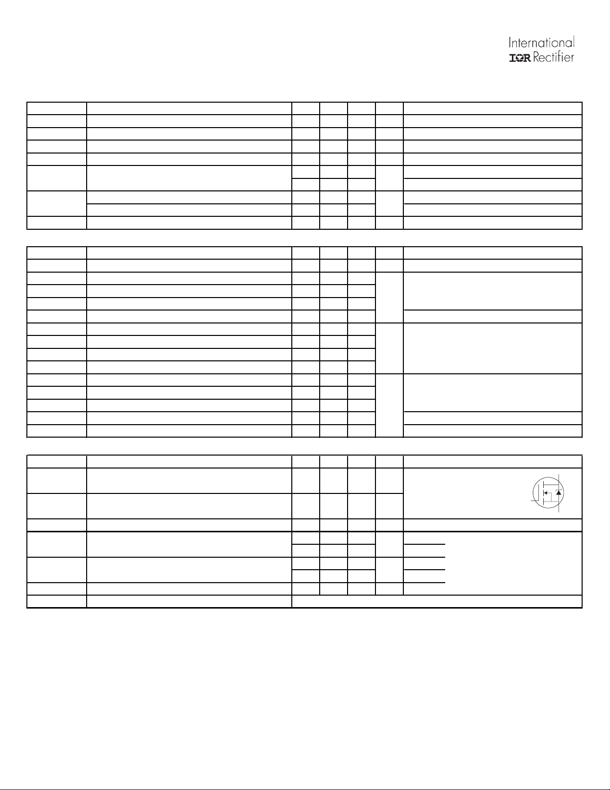
Static @ T
J
= 25°C (unless otherwise specified)
Symbol Parameter Min. Typ. Max. Units
V
(BR)DSS
Drain-to-Source Breakdown Voltage 40 ––– ––– V
∆V
(BR)DSS
/
∆T
J
Breakdown Voltage Temp. Coefficient ––– 0.037 ––– V/°C
R
DS(on)
Static Drain-to-Source On-Resistance ––– 1.4 1.75
mΩ
V
GS(th)
Gate Threshold Voltage 2.0 ––– 4.0 V
I
DSS
Drain-to-Source Leakage Current ––– ––– 20 µA
––– ––– 250
I
GSS
Gate-to-Source Forward Leakage ––– ––– 100 nA
Gate-to-Source Reverse Leakage ––– ––– -100
R
G
Internal Gate Resistance ––– 2.2 ––– Ω
Dynamic @ T
J
= 25°C (unless otherwise specified)
Symbol Parameter Min. Typ. Max. Units
gfs Forward Transconductance 1170 ––– ––– S
Q
g
Total Gate Charge ––– 160 240 nC
Q
gs
Gate-to-Source Charge ––– 40 –––
Q
gd
Gate-to-Drain ("Miller") Charge ––– 68 –––
Q
sync
Total Gate Charge Sync. (Q
g
- Q
gd
)
––– 92 –––
t
d(on)
Turn-On Delay Time ––– 23 ––– ns
t
r
Rise Time ––– 220 –––
t
d(off)
Turn-Off Delay Time ––– 90 –––
t
f
Fall Time ––– 130 –––
C
iss
Input Capacitance ––– 9200 ––– pF
C
oss
Output Capacitance ––– 2020 –––
C
rss
Reverse Transfer Capacitance ––– 1340 –––
C
oss
eff. (ER)
Effective Output Capacitance (Energy Related)
i
––– 2440 –––
C
oss
eff. (TR)
Effective Output Capacitance (Time Related)
h
––– 2690 –––
Diode Characteristics
Symbol Parameter Min. Typ. Max. Units
I
S
Continuous Source Current ––– –––
340
c
A
(Body Diode)
I
SM
Pulsed Source Current ––– ––– 1310 A
(Body Diode)
d
V
SD
Diode Forward Voltage ––– ––– 1.3 V
t
rr
Reverse Recovery Time ––– 27 ––– ns
T
J
= 25°C V
R
= 34V,
––– 31 –––
T
J
= 125°C I
F
= 195A
Q
rr
Reverse Recovery Charge ––– 18 ––– nC
T
J
= 25°C
di
/
dt
=
100A
/
µs
g
––– 41 –––
T
J
= 125°C
I
RRM
Reverse Recovery Current ––– 1.2 ––– A
T
J
= 25°C
t
on
Forward Turn-On Time Intrinsic turn-on time is negligible (turn-on is dominated by LS+LD)
I
D
= 195A
R
G
= 2.7Ω
V
GS
= 10V
g
V
DD
= 26V
I
D
= 187A, V
DS
=0V, V
GS
= 10V
T
J
= 25°C, I
S
= 195A, V
GS
= 0V
g
integral reverse
p-n junction diode.
Conditions
V
GS
= 0V, I
D
= 250µA
Reference to 25°C, I
D
= 5mA
d
V
GS
= 10V, I
D
= 195A
g
V
DS
= V
GS
, I
D
= 250µA
V
DS
= 40V, V
GS
= 0V
V
DS
= 40V, V
GS
= 0V, T
J
= 125°C
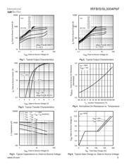
MOSFET symbol
showing the
V
DS
=20V
Conditions
V
GS
= 10V
g
V
GS
= 0V
V
DS
= 25V
ƒ = 1.0 MHz, See Fig. 5
V
GS
= 0V, V
DS
= 0V to 32V
i
, See Fig. 11
V
GS
= 0V, V
DS
= 0V to 32V
h
Conditions
V
DS
= 10V, I
D
= 195A
I
D
= 187A
V
GS
= 20V
V
GS
= -20V
器件 Datasheet 文档搜索
AiEMA 数据库涵盖高达 72,405,303 个元件的数据手册,每天更新 5,000 多个 PDF 文件
