Datasheet 搜索 > 接口芯片 > Intersil(英特矽尔) > ISL3179EFBZ 数据手册 > ISL3179EFBZ 数据手册 6/18 页

 器件3D模型
¥ 12.814
ISL3179EFBZ 数据手册 - Intersil(英特矽尔)
制造商:
Intersil(英特矽尔)
分类:
接口芯片
封装:
SOIC-8
描述:
INTERSIL ISL3179EFBZ 收发器, RS422 / RS485, 3V-3.6电源, SOIC-8
Pictures:
3D模型
符号图
焊盘图
引脚图
产品图
页面导航:
导航目录
ISL3179EFBZ数据手册
Page:
of 18 Go
若手册格式错乱,请下载阅览PDF原文件
ISL3179E, ISL3180E
6
FN6365.5
August 25, 2015
Submit Document Feedback
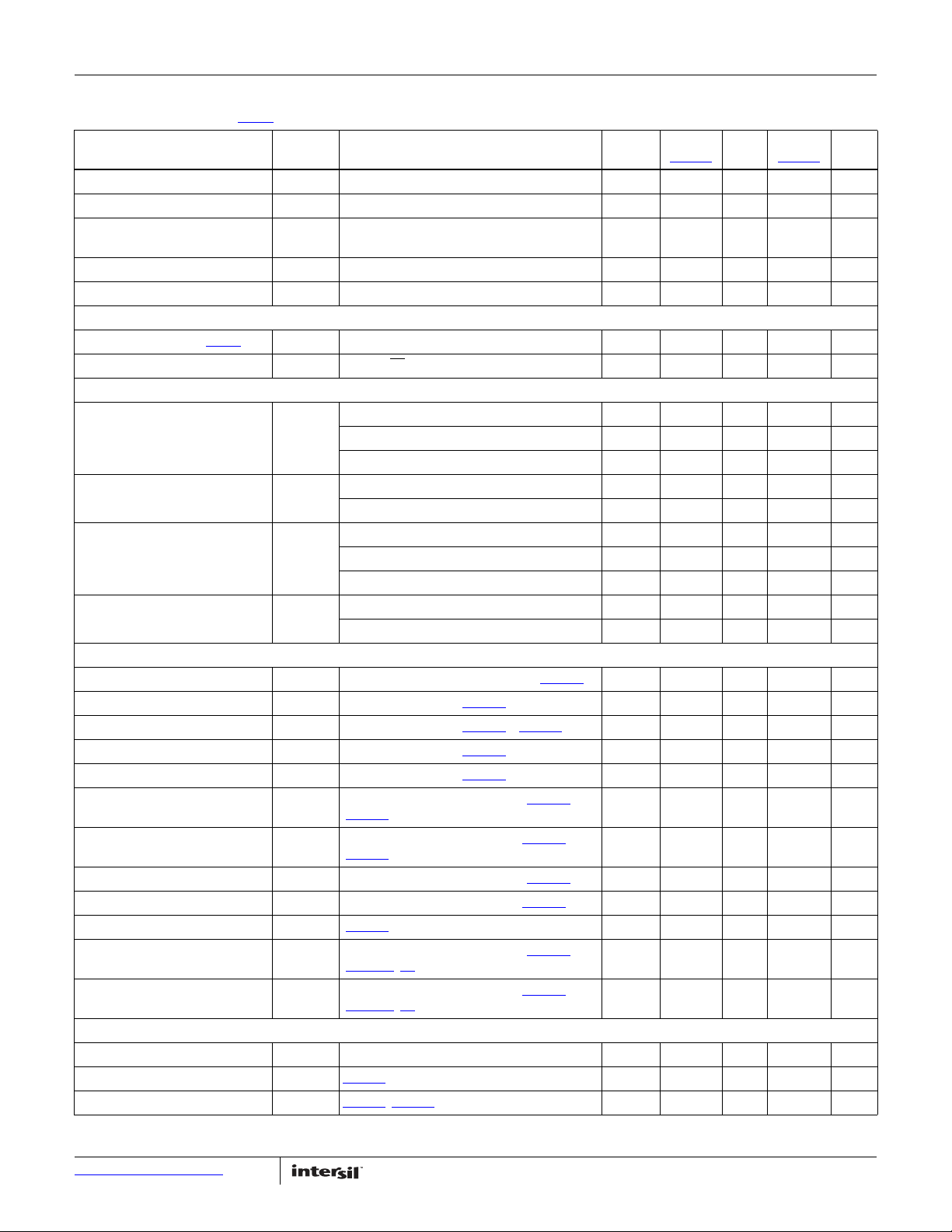
Receiver Output Low Voltage V
OL
I
O
= +10mA, V
ID
= -200mV Full - - 0.4 V
Receiver Output Low Current I
OL
V
OL
= 1V, V
ID
= -200mV Full 25 --mA
Three-state (high impedance)
Receiver Output Current
I
OZR
0.4V ≤ V
O
≤ 2.4V Full -1 0.015 1 µA
Receiver Input Resistance R
IN
-7V ≤ V
CM
≤ 12V Full 54 80 - kΩ
Receiver Short-circuit Current I
OSR
0V ≤ V
O
≤ V
CC
Full ±20 - ±110 mA
SUPPLY CURRENT
No-load Supply Current (Note 8
)I
CC
DI = DE = 0V or V
CC
Full - 2.6 4 mA
Shutdown Supply Current I
SHDN
DE = 0V, RE = V
CC
, DI = 0V or V
CC
Full - 0.05 1 µA
ESD PERFORMANCE
RS-485 Pins (A/Y, B/Z)
ISL3179E Only
IEC61000-4-2, Air-gap Discharge Method 25 - ±16.5 - kV
IEC61000-4-2, Contact Discharge Method 25 - ±9 - kV
Human Body Model, from bus pins to GND 25 - ±16.5 - kV
All Pins
ISL3179E Only
Human Body Model, per JEDEC 25 - >±9 - kV
Machine Model, per JEDEC 25 - >±400 - V
RS-485 Pins (A, B, Y, Z)
ISL3180E Only
IEC61000-4-2, Air-gap Discharge Method 25 - ±4 - kV
IEC61000-4-2, Contact Discharge Method 25 - ±5 - kV
Human Body Model, from bus pins to GND 25 - ±12 - kV
All Pins
ISL3180E Only
Human Body Model, per JEDEC 25 - ±3 - kV
Machine Model, per JEDEC 25 - ±150 - V
DRIVER SWITCHING CHARACTERISTICS
Maximum Data Rate f
MAX
V
OD
≥ ±1.5V, R
D
= 54Ω, C
L
= 100pF (Figure 7)Full 40 60 - Mbps
Driver Differential Output Delay t
DD
R
D
= 54Ω, C
D
= 50pF (Figure 5)Full-1116 ns
Prop Delay Part-to-part Skew t
SKP-P
R
D
= 54Ω, C
D
= 50pF (Figure 5), (Note 15)Full--4 ns
Driver Differential Output Skew t
SKEW
R
D
= 54Ω, C
D
= 50pF (Figure 5)Full-01.5 ns
Driver Differential Rise or Fall Time t
R
, t
F
R
D
= 54Ω, C
D
= 50pF (Figure 5)Full-47 ns
Driver Enable to Output High t
ZH
R
L
= 110Ω, C
L
= 50pF, SW = GND (Figure 6),
(Note 10
)
Full - 18 25 ns
Driver Enable to Output Low t
ZL
R
L
= 110Ω, C
L
= 50pF, SW = V
CC
(Figure 6),
(Note 10
)
Full - 16 25 ns
Driver Disable from Output High t
HZ
R
L
= 110Ω, C
L
= 50pF, SW = GND (Figure 6)Full-1525 ns
Driver Disable from Output Low t
LZ
R
L
= 110Ω, C
L
= 50pF, SW = V
CC
(Figure 6)Full-1825 ns
Time to Shutdown t
SHDN
(Note 12)Full60 - 600 ns
Driver Enable from Shutdown to
Output High
t
ZH(SHDN)
R
L
= 110Ω, C
L
= 50pF, SW = GND (Figure 6),
(Notes 12
, 13)
Full - - 1000 ns
Driver Enable from Shutdown to
Output Low
t
ZL(SHDN)
R
L
= 110Ω, C
L
= 50pF, SW = V
CC
(Figure 6),
(Notes 12
, 13)
Full - - 1000 ns
RECEIVER SWITCHING CHARACTERISTICS
Maximum Data Rate f
MAX
V
ID
= ±1.5V Full 40 60 - Mbps
Receiver Input to Output Delay t
PLH
, t
PHL
Figure 8 Full - 10 16.5 ns
Prop Delay Part-to-part Skew t
SKP-P
Figure 8, Note 15 Full - - 4 ns
Electrical Specifications Test Conditions: V
CC
= 3.0V to 3.6V; Typicals are at V
CC
= 3.3V, T
A
= +25°C. Boldface limits apply across the
operating temperature range. (Note 7
) (Continued)
PARAMETER SYMBOL TEST CONDITIONS
TEMP
(°C)
MIN
(Note 17
)TYP
MAX
(Note 17)UNIT
器件 Datasheet 文档搜索
AiEMA 数据库涵盖高达 72,405,303 个元件的数据手册,每天更新 5,000 多个 PDF 文件
